I did not try lower inpedances but sims by OP shows it works well. At higher output power same profile but THD increases a little and near clipping some higher orders appear H2//H3/H4/H5 but all monotonously decreasing and nothing above H5. I did not record any of these higher power tests so this is from my recollection.
The problem with multiple pairs is matching. Difficult to match four pairs; you would need at least 50 to select from, and you would have to measure them quickly to avoid thermal warmup, which hugely changes Vgs at the selected quiescent. A big pair of monsters is always better and there are some very good ones, like the IXYS 1040W devices. Here are 18 IXYS devices, Pmos and Nmos, with 90-140A and 960W to 1060W. All are suitable for your DLH, although you might want to reconsider the gate drive requirements carefully. These are designed for tractive/propulsive/smps application, I believe; but they move pretty quickly if you can move the charge into and out of the gate swiftly. These devices have outrageous transconductance, which is pretty good in linear operation as it reduces the compressive distortions.
Thanks very much Hugh for the great data!!!
I completely agree with you that pairing 4 pairs of mosfets is not an easy task. I'm not too attracted to designs whose output circuits are made up of several pairs of transistors. I have always tried to design circuits of relatively low power (for small listening environments).
The small original DLH (with a single pair of mosfets) has a huge virtue to exploit that is its own wide open-loop bandwidth (almost impossible to achieve with other well-known configurations, such as the classic 3-stage: LTP , VAS and EF). This allows to maintain very high resolutions up to very high frequency, without noticing too much the classic break in the distortion around 1 KHz.
The rare input circuit must maintain a delicate balance: on the one hand, avoid excessive self-heating of the two transistors that make up the input circuit; on the other hand, the current through the two transistors of the input circuit must be maintained in the plateau of the curve that describes the hFE with the collector current (to preserve the linearity); on the other hand, a certain slew rate must be reached, so that the current through the input circuit has a minimum value (value that also bears relation to the chosen type of mosfet and its interelectrodic capacities).
While it is tempting to use a single powerful output pair, my biggest fear with the IXYS are just their huge parasitic capacitors between their electrodes (ranging from 10nF to 23nF, approx.). Using 4 pairs of IRFP150N, the break in the OLG curve is significantly reduced in frequency by comparing it to the situation of a single pair of IRFP150N.
To mitigate the above, using higher power input transistors than the current signal transistors does not convince me, since they tend to be more limited in frequency and, in this way, I would be wasting the great possibility that the small DLH allows me.
I will continue analyzing it ...
The truth is that the small DLH can, with a very low complexity and practically without sophisticated technical resources, achieve amazing measurements, compared to other designs that require for the same between 4 to 5 times more components. The pressure on each piece of the DLH is very high (given its small number) and, its optimization, although in principle it seems simple is highly complex. It is a friendly circuit mostly with low closed loop gains, low voltages involved and his feedback network must operate very hot.
After 50 pages of the thread, you are making plans for pcb but there is no working proto? The circuit is very simple for point to point prototype.
I recommend reading carefully from the beginning of the thread, since there is enough and precise information to make an accurate assessment of the DLH. There are several simulations, real measurements and even innovative virtual evaluations. We must be at least 4 builders of the DLH. Good luck with your reading of these more than 500 posts !!!
 .
.No imd dim tim are shown so you like it fine but the underlying does are not shown, this is absurd.
No clipping point there are just not enough information audio specification were made for a reason.
Utterly absurd.
I recommend the same as a bogdan_borko, since much of the information requested is among these 500 posts.
Very rarely I heard an amplifier perform like this DLH (and I do not hold it for being its designer, but because it really fulfills what an outstanding amplifier should do)
Regards
Last edited:
Member
Joined 2009
Paid Member
diegomj1973 have a look Errata and Power Buffers
Broskie is often reinventing things that others have done before, adding a little spice and a great dialogue to go with which makes his blog one of the best ever for audio. Broskie has published on some similar circuits a few years back. Hugh Dean published a Rush Cascode + BJT output buffer a few years before that, buried somewhere in somebody else's thread. Nothing new under the sun is what I learned after I reinvented all sorts of stuff shortly after starting into this hobby myself
To my eyes diegomji1973's amplifier design is one of the more interesting variations and I really like the adjustability of the harmonic profile - not just a great learning tool but allow the amplifier to be more flexible in use.
Last edited:
The small original DLH (with a single pair of mosfets) has a huge virtue to exploit that is its own wide open-loop bandwidth (almost impossible to achieve with other well-known configurations, such as the classic 3-stage: LTP , VAS and EF).
It is not true. The classic 3-stage: LTP , VAS and EF (Blameless topology acording Douglash Self) is easy to have wide open-loop bandwidth using two pole compensation (TPC) or transitional miller compensation (TMC) or the other variations of two pole compensation, like which Dadod's discover.
Other topology such symmetry LTP input can use two pole compensation, too.
diegomj1973 have a look Errata and Power Buffers
Have you seen the date on which the blog was published?

I find that curiously striking ...
A lot of water has passed under the bridge since the DLH was presented ...
I do not discredit his blog, but he presents many of his schemes based on familiar circuits. I do not see anything new or innovative and, frankly, I do not think that many of their schemes have been physically implemented or tested. From a drawing of a circuital scheme to reality there is a long way and, many times, reality is very raw and daunting for every designer ...
Broskie is often reinventing things that others have done before, adding a little spice and a great dialogue to go with which makes his blog one of the best ever for audio. Broskie has published on some similar circuits a few years back. Hugh Dean published a Rush Cascode + BJT output buffer a few years before that, buried somewhere in somebody else's thread. Nothing new under the sun is what I learned after I reinvented all sorts of stuff shortly after starting into this hobby myself
To my eyes diegomji1973's amplifier design is one of the more interesting variations and I really like the adjustability of the harmonic profile - not just a great learning tool but allow the amplifier to be more flexible in use.
Many thanks!!!
It is not true. The classic 3-stage: LTP , VAS and EF (Blameless topology acording Douglash Self) is easy to have wide open-loop bandwidth using two pole compensation (TPC) or transitional miller compensation (TMC) or the other variations of two pole compensation, like which Dadod's discover.
Other topology such symmetry LTP input can use two pole compensation, too.

It would be interesting to show us if with similar complexity of scheme you would reach or exceed that parameter. You would need, at least, one more active element and a handful of passive components (crossing your fingers where nothing oscillates
)Best regards
Last edited:
The Achilles heel of your design is the limited output swing (and the practical consequences of it).
Offtopic, I was able to squeeze 11Vp-p output at 12V supply into 6 Ohm (resistive load so no real bragging rights here...) with a modified JLH69 topology (am not publishing it) built with pedestrian euro components (BC/BD transistors etc) at cca 400mA bias. IOW; "almost" R2R ...
Offtopic, I was able to squeeze 11Vp-p output at 12V supply into 6 Ohm (resistive load so no real bragging rights here...) with a modified JLH69 topology (am not publishing it) built with pedestrian euro components (BC/BD transistors etc) at cca 400mA bias. IOW; "almost" R2R ...
The Achilles heel of your design is the limited output swing (and the practical consequences of it)
The DLH does not have an Achilles heel ... it has a lot of them
!!!To mention just one of the many
: the shift of the DC offset with the temperature and its way of trying to correct it. Although for this defect there would be others possibles solutions: capacitive coupling to the speaker using a simple polarity power supply or running two units in bridge mode with direct output coupling.Best regards
Last edited:
offset drift remedy
Bias the input transistor with current rather than voltage . It needs to decrease as it heats up due to rise of beta and decrease of mosfet's bias voltage. The ntc mounted on the heat sink can do it . If the input transistor has a heat sink hence less beta increase it gives less variation .
Bias the input transistor with current rather than voltage . It needs to decrease as it heats up due to rise of beta and decrease of mosfet's bias voltage. The ntc mounted on the heat sink can do it . If the input transistor has a heat sink hence less beta increase it gives less variation .
Attachments
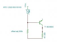
Thank you very much kokoriantz for your contribution! Any compensation attempt should counteract the voltage variation of the base-emitter junctions of the two bipolar transistors. The idea is that as the two joints heat up, the polarization potential of the base of the BC550C becomes less negative.
Best regards
Best regards
Member
Joined 2009
Paid Member
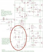
for me, because I could never accept the thinking of controlling current into base (as it relies on non-linear and rather inconsistent Hfe) I design with voltages and in all cases I can remember it's not difficult to insert a diode (or few) somewhere in the base circuit and put the diode and transistor into thermal contact. You can model it in LTSPice too, varying the temperature and watch to ensure temperature coefficient of idle current is negative and temperature coefficient of dc offset is relatively small.
for this amplifier you'll likely need more than 1 diode to match the temp.co for the dc-offset. In my TGM8 amplifier I used a single transistor wired up as a Vbe multiplier. It worked well although it takes more parts and you may prefer to keep it simple with a string of diodes type of approach. For my design, I fancied it up with a zener diode to create a steady fixed voltage off the negative rail so I didn't have to care too much about the rail voltage - you likely don't need that refinement. The Vbe multiplier is Q2 in the attached diagram and VR1 adjusts for the dc-offset (you'll need multi-turn or else split it into a variable + fixed resistors in series for more control).
There's many ways to skin this cat and you may find a different way that fits to the aesthetic you want.
Attachments
Last edited:
Thank you very much Bigun for your contribution !!! I agree with you.
The DLH with the compensation implemented with two bipolar transistors similar to those of the input circuit works very well and under very similar concept to which you have kindly exposed. In fact, that compensation was successfully tested by xrk971 and, probably, by others. In simulation, that compensation has also behaved well.
Best regards
Horacio
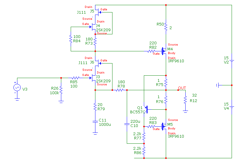
I just built TimS's amp, which in some ways reminds me of the DLH but it uses all JFETs on the front end. It has self-balancing DC offset. Tracks at 5mV hot or cold. The DC offset is controlled by matched J3 and J4 and identical R78/79.
My build here:
http://www.diyaudio.com/forums/head...e-performing-headphone-amp-5.html#post5453499
My build here:
http://www.diyaudio.com/forums/head...e-performing-headphone-amp-5.html#post5453499
- Home
- Amplifiers
- Solid State
- DLH Amplifier: The trilogy with PLH and JLH amps