The single supply amp is a small headphone amp Aksa and I developed. Headphones don’t like DC so it was a natural requirement and solution. The amp design is not public though - but basically take the design and shift the DC operating points such that what was formerly 0v (or GND), shift it to halfway between Vcc and 0v via adjustnents to resistor network in the Spice simulator. Then, AC couple the input and outputs.
The SMPS and filtering and cap Mx are discussed and described in the Aksa Lender Preamp thread and the ALPHA amp threads.
The SMPS and filtering and cap Mx are discussed and described in the Aksa Lender Preamp thread and the ALPHA amp threads.
Thanks for the reference XKR. Good P.S. reading.
I have a question more directly related to this thread. As I understand it, and please correct me if I'm wrong, the DC offset of an amplifier that runs off of a unipoler supply will change if the supply voltage changes, such as when the mains droops. Does an amp like the DLH suffer from this or does any residual DC offset remain constant?
I have a question more directly related to this thread. As I understand it, and please correct me if I'm wrong, the DC offset of an amplifier that runs off of a unipoler supply will change if the supply voltage changes, such as when the mains droops. Does an amp like the DLH suffer from this or does any residual DC offset remain constant?
I have a question more directly related to this thread. As I understand it, and please correct me if I'm wrong, the DC offset of an amplifier that runs off of a unipoler supply will change if the supply voltage changes, such as when the mains droops. Does an amp like the DLH suffer from this or does any residual DC offset remain constant?
To answer that question correctly, I will say that the DC offset depends strongly on the scheme we finally use.
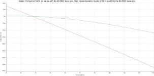
For example, the schematic of post 1 (the most basic of all) suffers from an important DC offset variation with the variation of the supply voltage.
For a nominal Vcc value of 15.67 V -> DC offset = + 149.361 uV (theoretical)
For a value of Vcc + 10% = 17.237 V -> DC offset = - 341.802 mV (theoretical)
For a value of Vcc - 10% = 14.103 V -> DC offset = + 334.415 mV (theoretical)
For example, the schematic of the post 13 (which has been compensated against the variation of the ambient temperature) does not suffer from significant DC offset variation with the variation of the supply voltage.
For a nominal Vcc value of 15.67 V -> DC offset = + 202.139 nV (theoretical)
For a value of Vcc + 10% = 17.237 V -> DC offset = - 33.928 mV (theoretical)
For a value of Vcc - 10% = 14.103 V -> DC offset = + 32,121 mV (theoretical)
All variations in the supply voltage suppose a variation of the current without signal (bias), unless the corresponding readjustments are executed to keep it within the design limits.
The DC offset values are the product of varying the rail voltages in a symmetrical way.
Best regards
PD: a great solution to these shifts would be to operate the outputs of two DLHs in a balanced way: goodbye DC offset, goodbye possible hum, welcome the most extraordinarily low levels of THD (possibly never reached by the best amplifiers built today).
Last edited:
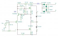
I built he dlh super buffer using this schema:
counter reaction network has been replaced by connecting the base of the BC550 to the output.
PP/SS and bias pots are 1Kohm
To have 1/2 Vcc at output (15v) had to set the ofset pot (at the base of BC560) to 850Kohm
now the input has high impedance, and simply attaching a big coupling capacitor influences the bias (it goes down)
what should I do? put an extra resistor from base of BC560 to Vcc?
both bc550 bc560 have hfe of 550
The value of the input signal coupling capacitor is correct (it would give very roughly a lower cutoff frequency of 0.125 Hz, or something around).
There are delays in the stabilization of final parameters, without applied signal, which will depend on the time constants involved in the circuit. Basically, in your circuit there will be two relatively important time constants: the conformed by the input network (approximately around 6.37 seconds, neglecting certain terms in its calculation) and another constant of around 23.5 seconds (again, approaching rudely).
To set idle parameters, remember to disconnect signal source and short-circuit the AC signal input to the DLHSB. Wait for the times mentioned between each readjustment, until reaching the final parameters.
It would not be strange that you have to finally modify the nominal value of the trimpot for DC offset, in the very basic configuration for the polarization of the base of the BC560C, since it is a configuration that depends a lot on the parameters of that same transistor.
The design was based on a transistor model with hFE of 330 (the one that was available in my library when designing it). You claim to have hFE of 550. It is for this reason that the relationship between the values of trimpots tends to be similar to the relationship between hFEs.
Although very basic, this configuration behaves better against offset shifts due to temperature, than a potentiometric divider of lesser value that polarizes the base of the BC560C.
If the DC shifts with the temperature are excessive with this basic configuration, you can implement the compensation with two transistors that has been tested by XRK971.
Attachments
Last edited:
Still using the simplified version with single psu rail and output cap.
Modified as follow:
Feedback network of 150r + 150r to ground without decoupling cap. 300k resistor at base of input trans to set the output at 1/2Vcc.
Will this affect performance? What would be the gain? 2X?
Modified as follow:
Feedback network of 150r + 150r to ground without decoupling cap. 300k resistor at base of input trans to set the output at 1/2Vcc.
Will this affect performance? What would be the gain? 2X?
If you have built a low gain DLH amplifier, but with a simple polarity power supply, you should add a capacitor in series to one of the two 150 ohm resistors of the feedback network (ie, in series with the resistor that connects with 0V). Otherwise, one of the resistors could dissipate up to about 431 mW in the absence of signal, for which both should preferably be at least 2 W.
It could work without that capacitor, only it will have a little more drift with the temperature and some more Johnson noise in the absence of signal (which could imply a very small decrease in the resolution of very low signal levels).
Remember that if you add a capacitor there, it should be of important value so as not to limit the response at low frequency.
Did you like the sound quality you get from DLH and DLHSB?
Have you played with the SE / PP setting?
Best regards
Last edited:
Compared to the super buffer Sound is more bright top end maybe a bit more aggressive.
Try placing a capacitor between 47pF to 68pF, in parallel to the 150 ohm resistor (which is connected between the node to the output and the base pin of the BC550C.) That should remove the "aggressiveness" at high frequency
") .
.Without that capacitor, a certain nonalignment in the high frequency response could occur.
As a reference, it would have to be connected in a similar way to the 82 pF capacitor in the schematic cited in post 1.
Last edited:
ok I will add a 47pf cap in parallel to the 150r that comes from the output.
I didn't used any electrolytic cap to decouple the 150r to ground.
is this ok?
I know that in this way dc current flows in the feedback resistors and noise is increased... but i didn't noticed any noise on the speakers
I didn't used any electrolytic cap to decouple the 150r to ground.
is this ok?
I know that in this way dc current flows in the feedback resistors and noise is increased... but i didn't noticed any noise on the speakers
About the electrolytic capacitor, there are no problems if you do not want to use it. Just consider what I said about the power dissipations in both 150 ohm resistors. They should be able to dissipate each one at least 2 W.
About the increase in Johnson's noise, it will surely occur at still imperceptible levels, even with very sensitive speakers. You have already verified this.
About the increase in Johnson's noise, it will surely occur at still imperceptible levels, even with very sensitive speakers. You have already verified this.
This is an other way of providing +/-15v output excursion.
I tested the irfp150 , at 250ma the simulated shows one A/V but measures in real world 0.45 .
Worst , the input capacitor datasheet values1.9n ,the simulator measures 3.9n. And still the model is provided by Tina ti .
Diegomj1973 , PRR mentioned about Christopher Rush created this circuit in 1964 . Have you found it . I looked in many on line technical libraries us archives ,the name is unknown to the profession. If such has existed in bipolar transistors, the output swing would be limited to +/-0.7v only instead of +/-4v with mosfet ,unless a remedy is applied , that PRR forgot to give notice .
Attachments
- Home
- Amplifiers
- Solid State
- DLH Amplifier: The trilogy with PLH and JLH amps