Glad to here your OnSemi parts were good. I tossed mine and bought Fairchilds. I was able to match 2 pair of each out of a dozen within 1%.
I too have my 120 back together just last night. Subjectively far improved.
New main caps, Hexfred rectifier, moved the VAS loading compensation to MC, selected correct gate stoppers for the Exicons, removed all other compensation except the feedback bypass which was necessary to tame the outputs. The slew is now symmetrical and about twice what it was, noise floor about 8 dB lower and line harmonics down by 12 dB. If I do another round, it will be a JFET IPS ccs and TMC with further additional C after the rail separation resistors. I may just leave well enough alone. It is quite a bit better. Bias is DOWN to 110. Now, my 220..... Starts out with a symmetrical topology. The MC boards were single ended IPS. I kind of agree with the textbook, it is the signal that needs to be symmetrical, not how you do it.
Stormrider: I refer you to your post #1032
I have an amp w/DC offset issues that uses those transistors. 2 or 3 each per channel in what I believe is a double-diff amp.
In the link below, see post #32 for a parts list; post #33 for a drawing .
http://www.diyaudio.com/forums/solid-state/177067-will-pay-belles-1-series-amp-info-schematic-4.html
thanks in advance, Tony
Are those MPS8099/8599 transistors still good? Are they matched?... This amp had MPS8099/8599 for the diff pairs,
I have an amp w/DC offset issues that uses those transistors. 2 or 3 each per channel in what I believe is a double-diff amp.
In the link below, see post #32 for a parts list; post #33 for a drawing .
http://www.diyaudio.com/forums/solid-state/177067-will-pay-belles-1-series-amp-info-schematic-4.html
thanks in advance, Tony
Last edited:
Hafler DH220 front-end voltage puzzler
Here's a strange situation:
After a voltage surge (lightning), the right channel of my Hafler DH220 had muted sound, as if the speaker fuse blew, but it was not that. The troubleshooting has been difficult (but interesting) for me, but I bet those that know this circuit would have some ideas and may find this puzzler interesting.
The amp was not on during the surge, and is plugged into a switched outlet. The surge probably worked its way through the earth lead.
Further complicating matters, I slipped with a probe and shorted two leads on Q1 (ccs for b+), and this caused some smoke on the pc board.
So, after that, I started from scratch, checking all components and replacing all of the transistors to be sure. Here is what I found:
Very low bias current (about 20mA), no surprise there. The MOSFETS checked out okay (checked gate-to-source voltage versus current). The power supply is okay.
1. Resistor R30 was burned, while R31 and R32 were low (36 and 40 ohms, instead of 47). I replaced all of these. All other resisters checked out okay, as well as the trimpots.
3. Checked all of the diodes, including the zeners, which I pulled to check the voltage. All okay.
4. Removed and checked all transisters on the board, and Q5 was broken (probably related to my shorting Q1). One lead on Q6 broke as I pulled it so I could not test it. All other transistors tested okay on beta and leakage. I ended up replacing them all gradually as I worked my way through the circuit. While I was at it, I matched every pair, even those not in the differential pairs.
5. After setting the DC offset (now < 5 mV), all of the voltages at the transistor leads were okay until I tested the collectors at Q8 and Q11. The collector voltage was +10 for Q8, and +7.5 for Q11. All the voltages at Q9 are off too (e,b,c = 7.5, 8.1, 10; should be -1.3, -0.6, 1.5)
The collector voltages at Q8 and Q11 should be about 1.5 and -1.4 volts, and as I understand it, the collector voltages here can increase, up to the 10 volt zeners, if there is a high load on the speakers and the feedback circuit tries to correct for it.
The other odd thing is at turn-on, the bias current is about 150 mV but drops exponentially to 20 mV (rapid, then gradually), as if there is some sort of load or leakage.
The voltages remain the same with the mosfets removed. I don't have a scope to look for ringing, but with the fets removed I think this is unlikely.
There is no signal on the input, and all the signal grounds are good, and no shorts anywhere in the wiring to the MOSFETS, speaker connectors, or the inputs. Checked for solder bridges.
5. Checked all of the electrolytic caps,and most of the film caps (only some bypass film caps skipped). All okay. Replaced the rail caps (100uf) caps and the feed-back cap (470uf) to be sure, as these are harder for me to test.
What could be causing the high voltages at Q8 and Q11 and the points beyond where expected (e.g., base at Q12 and Q13)? Why is there low bias current and voltage?
The gate voltages at the MOSFETS fluctuates close to zero (<15mV), and the source voltage is -25 for the N- and P-devices. Drain voltage is okay (+66 or - 66v). To be sure, I swapped in some other MOSFETS and problem persisted.
The hfe for the differential pairs is 95 to 105. Is this high enough and close enough?
Thanks in advance for any suggestions.
Perhaps this problem will improve our insight on the circuit, sort of like learning about the brain by studying damaged ones.
By the way, I put a new surge protector at the outlet, I get a lot of lightning here.
The manual contains a table of voltages expected at various parts in the circuit. Was it of any help in your troubleshooting?
Here's a strange situation:
After a voltage surge (lightning), the right channel of my Hafler DH220 had muted sound, as if the speaker fuse blew, but it was not that. The troubleshooting has been difficult (but interesting) for me, but I bet those that know this circuit would have some ideas and may find this puzzler interesting.
The amp was not on during the surge, and is plugged into a switched outlet. The surge probably worked its way through the earth lead.
Further complicating matters, I slipped with a probe and shorted two leads on Q1 (ccs for b+), and this caused some smoke on the pc board.
So, after that, I started from scratch, checking all components and replacing all of the transistors to be sure. Here is what I found:
Very low bias current (about 20mA), no surprise there. The MOSFETS checked out okay (checked gate-to-source voltage versus current). The power supply is okay.
1. Resistor R30 was burned, while R31 and R32 were low (36 and 40 ohms, instead of 47). I replaced all of these. All other resisters checked out okay, as well as the trimpots.
3. Checked all of the diodes, including the zeners, which I pulled to check the voltage. All okay.
4. Removed and checked all transisters on the board, and Q5 was broken (probably related to my shorting Q1). One lead on Q6 broke as I pulled it so I could not test it. All other transistors tested okay on beta and leakage. I ended up replacing them all gradually as I worked my way through the circuit. While I was at it, I matched every pair, even those not in the differential pairs.
5. After setting the DC offset (now < 5 mV), all of the voltages at the transistor leads were okay until I tested the collectors at Q8 and Q11. The collector voltage was +10 for Q8, and +7.5 for Q11. All the voltages at Q9 are off too (e,b,c = 7.5, 8.1, 10; should be -1.3, -0.6, 1.5)
The collector voltages at Q8 and Q11 should be about 1.5 and -1.4 volts, and as I understand it, the collector voltages here can increase, up to the 10 volt zeners, if there is a high load on the speakers and the feedback circuit tries to correct for it.
The other odd thing is at turn-on, the bias current is about 150 mV but drops exponentially to 20 mV (rapid, then gradually), as if there is some sort of load or leakage.
The voltages remain the same with the mosfets removed. I don't have a scope to look for ringing, but with the fets removed I think this is unlikely.
There is no signal on the input, and all the signal grounds are good, and no shorts anywhere in the wiring to the MOSFETS, speaker connectors, or the inputs. Checked for solder bridges.
5. Checked all of the electrolytic caps,and most of the film caps (only some bypass film caps skipped). All okay. Replaced the rail caps (100uf) caps and the feed-back cap (470uf) to be sure, as these are harder for me to test.
What could be causing the high voltages at Q8 and Q11 and the points beyond where expected (e.g., base at Q12 and Q13)? Why is there low bias current and voltage?
The gate voltages at the MOSFETS fluctuates close to zero (<15mV), and the source voltage is -25 for the N- and P-devices. Drain voltage is okay (+66 or - 66v). To be sure, I swapped in some other MOSFETS and problem persisted.
The hfe for the differential pairs is 95 to 105. Is this high enough and close enough?
Thanks in advance for any suggestions.
Perhaps this problem will improve our insight on the circuit, sort of like learning about the brain by studying damaged ones.
By the way, I put a new surge protector at the outlet, I get a lot of lightning here.
Thanks to tvrgeek and Dick West.
Would the feedback circuit be operating at all with no signal and the MOSFETS out of the circuit?
The outputs, if you mean the MOSFETS, don't get hot at all, as there is neglible bias current to them. The heat-sinked rivers on the board don't get very hot either -- I'd say they are at normal temperture (about 40 to 45 C).
And yes, I referred to the voltage chart in the manual, that's how I knew the voltages were okay up to Q7 and Q10. I also used the left channel voltages for reference too; some of these are slightly different than what is in the chart. As mentioned in the OP, the big deviations on the bad board are at Q8 and Q10 collectors and everything that follows those voltages.
Thanks again, tvrgeek.
Normally I would hesitate to remove the MOSFETS during testing, but what motivated me to remove them was a letter to Erno Borbely, published in the "Power Amp Projects" book (Audio Amateur Magazine, 1996). Borbely worked for Hafler and likley designed the DH200
The letter writer's amp, with a similar circuit as the DH200, was having ringing problems, and when the MOSFETS were removed during testing, the ringing stopped. In Erno's reply, there was no warning about removing MOSFETS. His advice centered around adjusting the capacitance around the MOSFETS.
Double-checking the caps near the MOSFETS would be worthwhile, but the point-to-point wiring has not changed, and the FETS are fine, so my guess is the problem is in the PC19 VAS board, but I am stumped as to what it is. Other posters mention the tendency for this amp to ring if improperly modified, but I had not changed anything on it in years.
I really wish you would come up with a solution to your PCB problem. I, too, have a DH-220 PCB that has, essentially, identical symptoms. I have no drive to the gates and the MOSFETs do not get warm but I have triple checked all voltages and everything seems to be in order, including MOSFET swaps to ascertain that they are functioning.
So . . . . I set this board aside 2 years ago intending to pick it up again and try a new approach. I am monitoring closely your trials and hope your eventual success might inspire me to give another go at my PCB. I hate to throw parts at something that otherwise seems to check out OK, but it seems I am down to having to try this. The final drivers (Q12 and Q13) will be the first pair on the replacement list (fingers crossed)and , as needed, will work back from there.
So . . . . I set this board aside 2 years ago intending to pick it up again and try a new approach. I am monitoring closely your trials and hope your eventual success might inspire me to give another go at my PCB. I hate to throw parts at something that otherwise seems to check out OK, but it seems I am down to having to try this. The final drivers (Q12 and Q13) will be the first pair on the replacement list (fingers crossed)and , as needed, will work back from there.
Many of the transistors cannot take full rail voltages and the currents when you have a failure. Changing one part at a time is not always useful. I would recommend pulling them out and measuring their gain on the bench. With the transistors out, you can check all the resistors.
Thanks again tvrgeek and eyoung,
I know my original post was long, but in it I explain that I tested the transistors (on a Heathkit IT-18, hfe and leakage) and ended up replacing them anyway, in pairs, except for Q9 which was replaced but is not paired with anything.
The voltage problem I am having has persisted after replacement, and I have re-checked several transistors, and the problem still remains. I also checked or replaced all of the 'litic caps, resisters and diodes, pulling the ones that needed it. As tvrgeek says, some of the volatges are a bit high for the device tolerances, so I could pull the transistors and test yet again.
One thing I have not tried is using high-beta transistors in the differential pairs (now they are about 100). I have some 2n5401 and 2n5550 in the 400 to 500 range. Erno Borbly recommended using diff. pairs in the 180 to 450 range range for his early version of the VAS similar to the Hafler. But his design did not have a trimmer for dc offset, and the design depended on reasonable matching and high hfe to keep the off-set low. I doubt this will make a difference, but will try anyway.
As Dick West mentions, problems can be hard to track down, and these boards seem fragile to me. I have had failed bias currents before, and Q9 is usually not the problem. I have never had one where the voltages check out but the MOSFTS have no bias current though -- that seems even more mysterious than what I have.
Working my way through this thread as I'll be getting a factory pair of DH200s tomorrow from a friend which I'll be setting up for vertical bi-amping. Parts are still in good condition, but simply due to age, I'll be changing out caps. My first mod will be changing both amps to 35A bridge rectifier ahead of installing new filter caps.
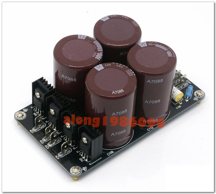
Has anyone tried installing a power supply board such as the below linked? It looks like it has two different halves, so it could feed both channels of the amp, with twice the factory capacitance in a tidy package.
4 10000uF 100V High Quality Power Supply Board for Power Amp DIY | eBay
Has anyone tried installing a power supply board such as the below linked? It looks like it has two different halves, so it could feed both channels of the amp, with twice the factory capacitance in a tidy package.
4 10000uF 100V High Quality Power Supply Board for Power Amp DIY | eBay
I have a DH200 sitting in front of me, and that board will only just barely fit mounted to the bottom of chassis. It might fit better mounted vertically.
You will probably need to add a softstart circuit. There is already a pretty large inrush spike with these amps with just the stock +/-10mF. You will kill the power switches, and stress the transformer and bridge rectifier(s) without something to limit the inrush current.
EDIT: Also, beware. There's a pretty good chance those caps are fake.
As with other recent posters, I am a little suspicious on the quality of the caps, as the board is so cheap. Also, it seems like the rectifiers on the board would be redundant with the bridge rectifier you plan on using. Why not just get decent 10k or (larger capacity if they fit) caps and use them as direct replacements for what is in the DH200? This would leave you the option of putting in a larger transformer in the future.
Then of course there are the driver boards that this thread has discussed in
depth.
A better switch and in-rush limiter are also a good ideas.
I have 40k uf of ps caps in my DH220 with a higher-rated switch, and have had no problems with the power supply (without an in-rush limiter) for many years. The last problem I had, with a blown-out driver board, happened when the amp was not even on (cause = lightning strike).
Good luck, and please let us know how the sound improves with veritical bi-amping.
- Home
- Amplifiers
- Solid State
- Hafler DH-200/220 Mods