My βeta Power Amplifier
Hi,
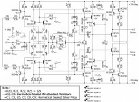
My βeta power amplifier is inspired by a lot of symmetrical VFB amplifer like HK990, Chriss Ovation E-amp... and the legend Leach amp (of course!). The output stage is encouraged by Pavel Macura.
Since my amp still in paper (HDD for sure) and in -βeta stage, so I think there must be a lot of "bugs" to "de" Please help me to spot and "de" them
Thanks all!
Hi,
My βeta power amplifier is inspired by a lot of symmetrical VFB amplifer like HK990, Chriss Ovation E-amp... and the legend Leach amp (of course!). The output stage is encouraged by Pavel Macura.
Since my amp still in paper (HDD for sure) and in -βeta stage, so I think there must be a lot of "bugs" to "de"
Please help me to spot and "de" them Thanks all!
Attachments
Last edited:
Looks good so far. Those TO3 output devices are a bit old school but should work well.
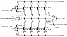
MJ21195/21196 is the cheapest in high power BJT family, and almost the toughest
Are T9/12 correct?
Are T10/13 a pair of folded cascode?
I am not keen on your DC offset adjust.
Have a look at the Krell version (and some others) that use a pair of signal diodes across the 10k to reduce the limits of adjustment.
Add a lot of RC filtering.
Change the upper leg of the NFB from paralleled resistors to series connected resistors.
The closer the value of the resistors in the upper leg to the lower leg resistor the more you remove resistor distortions from the output. And aim for the highest dissipation (at maximum output) to be <10% of the feedback resistor power rating.
Add a lot more supply rail decoupling.
at least some dedidcated to the main outputs, maybe two pair shared between the 8 devices.
Possibly some at the driver collectors.
Probably dual decoupling at the VAS and again at the Input.
All the HF decoupling MUST have low inductance routes for the transients currents to return to the capacitors. The capacitor is the source of transient current and must RETURN to that source. It's not enough for the flow route to be short, the total route must be short. This will determine the PCB layout.
Consider an LED in the D1 to D4 string.
and also in the R26 string & R34 string.
green indicators give confirmation of OK operation.
Add power diodes across R2 (1n4001 seem to be good enough).
There is nothing wrong with R1=10k
But if you have a few channels all @ 10k being driven by a source, the currents start getting a bit high.
And requires a big capacitor for your DC blocker.
Consider placing 100k here and add a pair of spare pads to adjust if needed.
The bias currents from the two inputs will be very low and thus the voltage offset here will also be low.
place pads for a series resistor in the C2/3 routes.
Last edited:
Are T9/12 correct?
Are T10/13 a pair of folded cascode?
I am not keen on your DC offset adjust.
Have a look at the Krell version (and some others) that use a pair of signal diodes across the 10k to reduce the limits of adjustment.
Add a lot of RC filtering.
Change the upper leg of the NFB from paralleled resistors to series connected resistors.
The closer the value of the resistors in the upper leg to the lower leg resistor the more you remove resistor distortions from the output. And aim for the highest dissipation (at maximum output) to be <10% of the feedback resistor power rating.
Add a lot more supply rail decoupling.
at least some dedidcated to the main outputs, maybe two pair shared between the 8 devices.
Possibly some at the driver collectors.
Probably dual decoupling at the VAS and again at the Input.
All the HF decoupling MUST have low inductance routes for the transients currents to return to the capacitors. The capacitor is the source of transient current and must RETURN to that source. It's not enough for the flow route to be short, the total route must be short. This will determine the PCB layout.
Consider an LED in the D1 to D4 string.
and also in the R26 string & R34 string.
green indicators give confirmation of OK operation.
Add power diodes across R2 (1n4001 seem to be good enough).
There is nothing wrong with R1=10k
But if you have a few channels all @ 10k being driven by a source, the currents start getting a bit high.
And requires a big capacitor for your DC blocker.
Consider placing 100k here and add a pair of spare pads to adjust if needed.
The bias currents from the two inputs will be very low and thus the voltage offset here will also be low.
Add pads for a series resistor in the C2/3 routes.
Add pads for base stoppers to the drivers and the outputs.
Are T9/12 correct?
Are T10/13 a pair of folded cascode?
I am not keen on your DC offset adjust.
Have a look at the Krell version (and some others) that use a pair of signal diodes across the 10k to reduce the limits of adjustment.
Add a lot of RC filtering.
Change the upper leg of the NFB from paralleled resistors to series connected resistors.
The closer the value of the resistors in the upper leg to the lower leg resistor the more you remove resistor distortions from the output. And aim for the highest dissipation (at maximum output) to be <10% of the feedback resistor power rating.
Add a lot more supply rail decoupling.
at least some dedidcated to the main outputs, maybe two pair shared between the 8 devices.
Possibly some at the driver collectors.
Probably dual decoupling at the VAS and again at the Input.
All the HF decoupling MUST have low inductance routes for the transients currents to return to the capacitors. The capacitor is the source of transient current and must RETURN to that source. It's not enough for the flow route to be short, the total route must be short. This will determine the PCB layout.
Consider an LED in the D1 to D4 string.
and also in the R26 string & R34 string.
green indicators give confirmation of OK operation.
Add power diodes across R2 (1n4001 seem to be good enough).
There is nothing wrong with R1=10k
But if you have a few channels all @ 10k being driven by a source, the currents start getting a bit high.
And requires a big capacitor for your DC blocker.
Consider placing 100k here and add a pair of spare pads to adjust if needed.
The bias currents from the two inputs will be very low and thus the voltage offset here will also be low.
Add pads for a series resistor in the C2/3 routes.
Add pads for base stoppers to the drivers and the outputs.
Thanks for comment.
- T9/12 and T10/13 like what you seen.
- I will add the diode to DC offset trimmer, great benefit indeed!
- About all decoupling problems:
+ Some decoupling haven't been included yet, since I haven't draw a package for them. I will use PIO and polycarbonate for decoupling cap (which are not in library) because I have a bucket of them.
+ The supply voltages for LTP and VAS stages are regulated so heavily decoupling seem not neccessary. All tracks/connecting wires will be kept as short as possible since they are one of the most important task in sensitive analog circuit.
+ Output stage using point-to-point configuration so decoupling are easily added. I choose 90V 10uF tantalum for this task.
- Can you tell me more about choose resistor value/config in NFB?
- Why LED and 1N4001?
- I don't think I will have problem with 10k input resistor and no DC blocker
- I will add base stopper and true snubber network.
- Status
- This old topic is closed. If you want to reopen this topic, contact a moderator using the "Report Post" button.