Picked up a Hafler P-500 on the cheap. The guy said the unit kept blowing "some fuses". I figured for $50 bucks I could give it a whirl.
Well as expected a lot was wrong with the amp. I have done a total recap and replacement of several resistors, diodes and a couple fried transistors. Right now I am just working on one channel then tackling the second after. The channel I am currently working on is producing music with an offset of ~6mV but I am having trouble with a few of the voltages and setting the bias. I replaced the bias transistor with 2N5550. It should be a NP2222A but I read that a decent NPN should suffice. Q13 was also changed as it was fried.
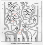
I attached a pic of the test points and the values I am getting. All other test points are correct. When I try and adjust the bias I am only able to get around 140mV across the fuse then the relay kicks in and the fan stops. If I drop below this everything kicks back on and I am able to produce sound.
I just realized as I was writing this that the I still had the unit on the dim bulb during biasing and that may be the reason for the erroneous values. I will see what I get tomorrow without the dim bulb.
Either way I would appreciate any help.
Well as expected a lot was wrong with the amp. I have done a total recap and replacement of several resistors, diodes and a couple fried transistors. Right now I am just working on one channel then tackling the second after. The channel I am currently working on is producing music with an offset of ~6mV but I am having trouble with a few of the voltages and setting the bias. I replaced the bias transistor with 2N5550. It should be a NP2222A but I read that a decent NPN should suffice. Q13 was also changed as it was fried.
I attached a pic of the test points and the values I am getting. All other test points are correct. When I try and adjust the bias I am only able to get around 140mV across the fuse then the relay kicks in and the fan stops. If I drop below this everything kicks back on and I am able to produce sound.
I just realized as I was writing this that the I still had the unit on the dim bulb during biasing and that may be the reason for the erroneous values. I will see what I get tomorrow without the dim bulb.
Either way I would appreciate any help.
Attachments
Last edited:
Just realized the voltages in red surrounding Q13 should be negative.
Another update: I removed the dim bulb and brought the unit back up on the variac. No issues and the relayed clicked on as expected. I am still getting the same voltages as shown in the above pic. The bias amperage remains low and although it can be adjusted, I can't get it to the specified value (350mA).
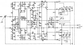
I am thinking this inability to bias is most likely due to the lower negative voltage feeding into the bias circuitry. Q9 appears to functioning appropriately as the voltage change is correct. Looking at the schematic the only other parts involved would be D10 (replaced already), Q11/Q13 (working) and D13/D14 (replaced D13 but not D14).
I am going to replace D14. The amp sounds fine to my ears although I haven't hooked up the scope to check signal waveforms. Definitely scratching my head with this one.
Another update: I removed the dim bulb and brought the unit back up on the variac. No issues and the relayed clicked on as expected. I am still getting the same voltages as shown in the above pic. The bias amperage remains low and although it can be adjusted, I can't get it to the specified value (350mA).
I am thinking this inability to bias is most likely due to the lower negative voltage feeding into the bias circuitry. Q9 appears to functioning appropriately as the voltage change is correct. Looking at the schematic the only other parts involved would be D10 (replaced already), Q11/Q13 (working) and D13/D14 (replaced D13 but not D14).
I am going to replace D14. The amp sounds fine to my ears although I haven't hooked up the scope to check signal waveforms. Definitely scratching my head with this one.
For $50 you did OK as long as the output FETs are good. Since the negative driver transistor, Q13, has a + voltage on it's base it is OFF and therefore the negative outputs are OFF too, OFF means no current. Find out why Q13's base is positive and it should be fixed. An o'scope will reveal all signal wise, I'll bet you have no - going signal on the output.
Craig
Craig
I made a mistake with the voltages around Q13. They are appropriately negative. I am working on changing the attachment above.
I do get sound out of the amp and it actually sounds fine (no obvious distortion). My main issue is the inability to bias the amp along with the wrong voltages surrounding Q9/11/13.
Sorry for the confusion
I do get sound out of the amp and it actually sounds fine (no obvious distortion). My main issue is the inability to bias the amp along with the wrong voltages surrounding Q9/11/13.
Sorry for the confusion
Since this circuit is symmetrical what you have on the + side you should have on the - side but opposite polarity. Each pair of Q7/Q10, Q8/Q11, and Q12/13 should have the same voltages on their EBC. C6 should have the same voltage on both sides referenced to ground but again opposite polarity. The bias circuit is basically an adjustable Zener diode. The setting of P2 sets the conduction of Q9, the harder Q9 conducts the less voltage across C6 and the lower output stage current and vice versa. Find where you loose voltage symmetry. Exactly what parts were bad and what did you replace them with?
Craig
Craig
Thanks for the help llwht.
I will double check the voltages to confirm but if I recall correctly all the listed transistors have equal (albeit opposite) voltages feeding into them. The difference occurs between the Q11 collector and Q13 base. On the negative rail it is the -0.765V and on the positive it is +1.16V. Documented value is 1.2V. This is where the difference begins and this also translates to the emitter of Q13 being -0.140V on the negative side. The -0.765 and +1.16 also corresponds to what you were referring to in regards to C6.
What I have changed so far:
- D12, D13, D15, D16 with exact replacements
- Q8/Q11/Q12/Q13 with exact replacements (one was fried so I did all of them)
- Q9 with a 2n5550 after I was having trouble with bias and thought this was suspect.
- Several resistors that either had heat damage or were carbon comp. Replaced with metal film 5%. I checked all to confirm appropriate ohm reading.
I understand the voltage symmetry and I know it is somewhere between Q11/13 but I am having trouble determining where. Only other connected parts are D14 and the resistors around Q9. That's where I will focus next and confirm I am gooding good voltages feeding into the transistors as recommended.
Thanks again for the help
Good score on that amp, hope you can get it sorted out soon.
I thought so. My father actually snagged this one after calling me and asking if it was a decent deal. I told him yes as fast as possible! Anyways, when I get it up and running, it is going back to him for his garage speakers. He runs 4 Bose 901 that the neighbors love
 . This will replace a Phase Linear 700 series I which will be getting a complete makeover once the replacement amp is up and running.
Hi phase, that would be awesome but That is probably in mono. We would probably get more than the stated 255 WPC running two speakers one each side for a total of 4 ohms.
Craig, thanks for the clever idea to short C6. I'll give it a try and see if it narrows down the problem.
Craig, thanks for the clever idea to short C6. I'll give it a try and see if it narrows down the problem.
Craig,
I shorted C6 as you advised. I am now reading 0.440V at C6. If I am interpreting this correctly I should actually have close to 0V as the positive/negative rails are symmetrical and should cancel each other out. This also means I am missing -0.440V on the negative rail which is consistent with my previous readings. Only difference now is the bias has been bi-passed and is probably not responsible for my issues.
I also checked the other test points and everything is essentially spot on with the schematic and equal in comparison to the negative/positive sides.
I am going to double check some resistors but I am putting my money on D13 or D14.
Thanks again for the tip on circumventing the bias. That seems to have saved me quite a bit of troubleshooting.
I replaced the !n4148 diode on both sides and double checked the 4 diodes because I thought maybe the polarities were off. Based on the screening they are OK. Didn't think of it at the time but I will double check the traces to confirm what is screened on the board in regards to polarity is consistent with the actual layout.
After replacement I am still getting +0.440V so I didn't change anything. I am going to check all the resistors again to see if any are off. They weren't before but at this point I might have missed something.
I did notice some slight differences in voltages at D8 and D7 away from test point E were different. D8 was -.642V and D7 was +0.617. I am going to finish replacing diodes but I can't imagine those values causing my problem.
- Q8/Q11/Q12/Q13 with exact replacements (one was fried so I did all of them)
Which one was fried ?
Failure mode CE open ?
R29: -1.5V (this is the same but positive on the other side)
R30: -1V (also the same but positive on the other side)
I got this value by subtracting each leg in relation to ground
Q13 was the dead transistor. The base leg was fried off and fell out when I desoldered the lead.
R30: -1V (also the same but positive on the other side)
I got this value by subtracting each leg in relation to ground
Q13 was the dead transistor. The base leg was fried off and fell out when I desoldered the lead.
Last edited:
- Status
- This old topic is closed. If you want to reopen this topic, contact a moderator using the "Report Post" button.
- Home
- Amplifiers
- Solid State
- Hafler P-500 Restoration