")

If you can live with three more transistors, You can consider mike Reynardson Mjr7. Lateral fet ops and op cap. Bulletproof and way better than those Maplin 50w kits people used as guitar and pa amps......
MJR7-Mk5 Mosfet Power Amplifier
MJR7-Mk5 Mosfet Power Amplifier
Hi
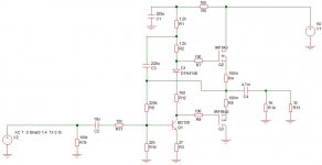
You should try something like this (see file)
Of course, Q2 and Q3 on heatsink,
R10 should be a pot to tune to Valim/2 (here V1/2) the voltage between R4 or R5 to ground,
R12 must be a pot to tune the MOS current between 50 to 100mA (5 to 10 mV at R4 or R5),
D1 should be in contact with the MOSFET heatsink,
R14 and R15 are just here to set the voltage of the capacitor when nothing is connected at the input or output.
I just have done simulations.
Regards
Attachments
GChap... Take a look at #8...
http://www.diyaudio.com/forums/solid-state/308770-simple-class-b-ab-mosfet-amp.html#post5102476
http://www.diyaudio.com/forums/solid-state/308770-simple-class-b-ab-mosfet-amp.html#post5102476
R1 could be increased, but not more than 1/3 of R2, that is how i see good bootstrapping.
R4 needs to be small because of R5's value, low ohm values there lessens the influence of the base impedance wich is not fixed but varies with signal.
R6 need to be small because of the total base impedance wich is low, a bigger R6 would require a much bigger signal to drive the amp.
R3 and C6 increase the AC negative feedback, thus the THD is reduced ( in my simulations by more than half ).
I have already said, the zener could be replaced with a few 4148 diodes ( the more, the better ), wich if fixed on the heatsink can give some form of thermal compensation for the bias. This would require a different value for R11 ( trim-resistor ) wich sets the bias.
Last edited:
To my opinion,
R1, R4 and R6 are too small,
R3 and C6 are useless,
and I don't remember the sign of a zener thermal coef, and I would suppress it, which makes R11 too small.
But may be I'm wrong
which schematic in which post are you two discussing?R1 could be increased, but not more than 1/3 of R2, that is how i see good bootstrapping.
R4 needs to be small because of R5's value, low ohm values there lessens the influence of the base impedance wich is not fixed but varies with signal.
R6 need to be small because of the total base impedance wich is low, a bigger R6 would require a much bigger signal to drive the amp.
R3 and C6 increase the AC negative feedback, thus the THD is reduced ( in my simulations by more than half ).
I have already said, the zener could be replaced with a few 4148 diodes ( the more, the better ), wich if fixed on the heatsink can give some form of thermal compensation for the bias. This would require a different value for R11 ( trim-resistor ) wich sets the bias.
Hi. I am locking for a schematic of a simple class B or AB mosfet amplifier.
I found one which I thought was the ideal, with IRF540/IRF9540, but it does not work.
Someone knows a schematic of a simple (1~2 transistors + 2 mosfet - preferably IRF) class B or AB mosfet amplifier that works? 20~30W is enought.
The use is for guitar.
Thanks.
I have designed and simulated a circuit according to your needs.

It is almost as simple as yours. 1 transistor more is needed for a Darlington pair to get the required current gain for a useful high input resistance.
- Home
- Amplifiers
- Solid State
- Simple Class B or AB Mosfet Amp