Lisandro_P
You could create a negative reference of two forward baised diodes and put a trim pot across them. Connect the 47K input resistor to the wiper of this pot and you can pull the base down so that emmiter is sitting just below ground. The pot can be nulled for zero offset at output. You really might want to ac couple the feedback resistor to ground since the DC offset is going to drift on this thing. Especially without the benifit of a long tailed pair diff amp for a front end.
H.H.
Harry's suggestion will work and was in fact used on yet another version of the JLH Class-A, the Class-A headphone amp published in Hi-Fi News Jan/Feb 1979. If this method is used, the polarity of the feedback capacitor to ground will need to be reversed since the emitter of Tr4 will sit at -0.65V as opposed to +0.65V for the 7815/ccs method. A 100uF capacitor across the diodes will also be beneficial.
The dc offset variation with supply rail voltage and/or temperature will be greater with the diode/resistor arrangement than it is with the 7815/ccs. I quote from another JLH article for a 270W/4ohm amp that uses a similar input stage and NO capacitor in the feedback leg to ground:
" In order to minimise the effect of common mode distortion at the input, while preserving the facility of a direct coupled structure, the customary ' long- tailed pair' has been replaced by a single transistor, in which the offset which would otherwise arise due to its base-emitter voltage and the emitter circuit current flow through the feedback resistor, is removed by an additional current source employed to inject a sufficient quantity of current into the emitter of the input transistor to offset this voltage. Again, since the input transistor remains at ambient temperature, the constant current source can be arranged to track this thermally, and remove errors in dc offset due to ambient temperature changes."
Geoff
Base bias
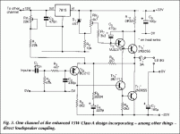
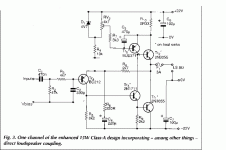
Since I did a bit of a poor job explaining...... In reference to the schematic below. The quiesent current of TR4 is about 1.3 volts divided by 8.2K ohms or 0.16mA. With a cap (to ground) connected to R6 and no current source, the only DC path is though R8. The output is sitting at 0 volts, so the emmiter should be at about -0.16mA multiplied by 2.7K or -0.43 volts. This neglects the base current of Tr4 through the 47K resistor which is small and could be nulled out. The bias for the -1.3 volt reference could be supplied by a JFET current source for good noise rejection and stability with changing supply voltages. R2 could be connected to the wiper of a 10K ohm trim pot across the negative 1.3 volt reference. An LED could be used for a reference also since the base voltage is being adjusted the trim pot. The exact reference voltage is not critical as long as it is stable and low noise. A green LED would give about -1.85 volts. I think the temperature stability should be fine.
H.H.
Attachments
As I said in my last post, this has been done before. See Circuit 1 at:
http://www.gmweb.btinternet.co.uk/jlhphones.htm
As Harry has suggested, R3 in Circuit 1 can usefully be replaced with a Jfet ccs or similar and a pot can be incorporated to provide a means of adjustment.
Geoff
http://www.gmweb.btinternet.co.uk/jlhphones.htm
As Harry has suggested, R3 in Circuit 1 can usefully be replaced with a Jfet ccs or similar and a pot can be incorporated to provide a means of adjustment.
Geoff
again a bit more in depth with this schematic
I discussed the schematic with a friend and he suggested that R9 is a source of some of the distortion. There is a current flowing from Tr4 to Tr3 to Tr1 which changes with audio signal, but it's not linear and because of that there forms a small voltage on R9 that adds to the output signal and also is not linear. As far as I understand it should be possible to leave this resitor out.... Do you guys see any possible problems with that and consider it worth exploring?
**
Geoff, do you know if anyone has tried to use some other method than Tr5 current source in JLH'96 or the original resitor current source? This is the point that troubles my mind the most and I would like to think through any possible solution and then try the few most appealing.
Ergo
scottnixon, could you please mail the Bedini circuit to me too. It interests me, because I have one project of my own design that has the same front end but I ran in trouble with output and stability. This I quess would give ideas how to do it a bit different ")
My mail is ergo.esken@mail.ee
Ergo
My mail is ergo.esken@mail.ee
Ergo
I have asked Geoff about the R9 also some time ago... I did that because Rod Elliot made a observation that a high R9 has more distorion but only second harmonic, and low R9 has lower distortion but mainly third harmonic...
My simulator show give any differnce
so .......????? I don't get it...
greetings,
thijs
My simulator show give any differnce
so .......????? I don't get it...
greetings,
thijs
Ergo, Thijs
I would not omit R9. I think the comment regarding distortion/R9 value that Thijs is referring to is the one Rod made in relation to one of his prototypes for the DoZ. This was not the JLH circuit but was a Darlington output transistor with a resistive collector load. Rod found that with no base resistor for the Darlington, the distortion was predominantly 2nd harmonic but was three times higher than when a base resistor was fitted. With the base resistor, the distortion was mainly 3rd Harmonic.
Of more importance, without a base resistor the positive going slew rate was degraded due to the lack of a base discharge path which resulted in severe degradation of the leading edge of a 10kHz square wave.
A similar situation will exist for Tr1 in the JLH circuit so I suggest that R9 remains, though I don't think its value is too critical.
I'm afraid I don't follow Ergo's friend's line of reasoning but I will give it some more consideration over the weekend. My initial thought is that the voltage across R9 (and hense the current through it) is determined by the Vbe of Tr1. This will vary with the collector current of Tr1 and with its c-e voltage. Indulging in a little speculation, pehaps what is required here is a transistor with a linear variation of Vbe with collector current (since it is not possible to obtain a device with no variation). Comparing the Vbe/Ic characteristic for an MLJ3281a with that of the MJL21194 over the operating range of current (say 0.1A to 2.5A) will show what I mean.
Ergo, I agree with your reservations about Tr5. Simulation shows that distortion with the Tr5 circuit is about twice that of an ideal current source or even the 1969 bootstrap arrangement. If you want to avoid Tr5, the ccs shown in the outline schematic in my previous post can be a standard two-transistor or LED/transistor circuit. An alternative is to revert to the 1969 bootstrap arrangement. As explained by Hugh Dean in another thread, the stability of the amp should be better with the bootstrap since the high frequency performance of the bootstrap capacitor will cause the gain of Tr3 to be reduced at higher frequencies thus improving the phase margin. There is some empirical evidence of this in that a 1969 version of the JLH worked using 2SC3281 output transistors whereas a 1996 version using the MJL3281a oscillated.
Again I will quote JLH from another of his articles:
"Relatively few design decisions now remained. Of these, the most significant was whether to give the second, class-A amplifier stage a bootstrapped collector load or to use a constant current source. The merits of these two arrangements are fairly well balanced. For example, the bootstrapped driver will give a slightly larger output power for the same HT voltage, and is simpler, while the constant current source arrangement will give a slightly lower second harmonic distortion figure which allows the same overall THD figure to be obtained with a lower open-loop gain - which makes the preceding circuitry simpler"
The input stage referred to in this quote was basically the same as that in the Class-A design. My simulations of the Class-A indicate that there is very little difference in THD between the ccs and the bootstrap except at very low frequencies, where the bootstrap capacitor begins to loose its effectiveness and the distortion rises a little.
Geoff
JLH
Thanks Geoff for your very detailed analysis. I too feel the use of a constant current source for the positive leg of the output is the way to go. This the arangement that I prefer for my Aleph 3. It was not in jest that I said that the JLH topology shares some resemblance to that of the Aleph series. Perhaps a hybrid of Fet and BJT transistors would be interresting. A 2SJ74 p channel Jfet with CCCS might even allow direct coulpling for the amp. Also an IRF 510 for the driver of the output BJT would be interesting......
H.H.

And you won't....
Gate resistors or the thing will oscillate. IRFP 240 on outputs, IRF510s won't last long for a power amplifiers and don't have enough transconductance. The source resistors for output Mosfets should be at least 0.5 ohms for bias stability. Some kind of current limiter or fuse is a real good idea. Everybody simulates..... doesn't anyone actually build something?
H.H.
yeh yeh yeh... I know... I was just playing around.. I did make such remarks on my first post... but heee.. you askes for it ..
so don't be smart with me boy..
The funny thing is that it simulated so good... very linear.. and good bandwidth (also because of high Iq of the driver stage) I still think it might be something nice to try someday... transductance is good enough of high lineairity.. You may be right about the 0.1R being to low but the negative temperature coefficient helps in this case...The Iq is 1.2Amps is this case and so current is limited allready (???? or is it not?)
And heeeeee .. This thread started with my latest finished project!
You only build passive preamps.. my guinea pigs can do that
Thijs
It is not....
Anybody can get an amp to work with a spice model, reality places other costraints on the design. Iq has nothing to do with current limit. At over 17 watts dissapation, an IRF 510 won't last long. Mosfets oscillate without gate resistors. Like I said, a man has to know his limitations.... I have posted pictures of two amp designs, a modified Aleph 3, a jfet buffer, and several very good passive preamps. Do your guinea pigs do spice modeling also?
H.H.
- Home
- Amplifiers
- Solid State
- JLH 10 Watt class A amplifier