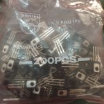
I've used BD139's in several amplifiers with good results.
There may be some "out there" which don't have a high ft - there was a similar range BD239 which are epitaxial base 3MHz-ish. If there are slow BD139's they're likely fakes. Measurement I've made on ST and ON Semi seem to suggest 100MHz+. Philips made the original devices, I believe, and they're over 100MHz as well. But Philips offloaded their semi manufacturing to NXP. The NXP datasheet shows typical gains around 150. I don't think Philips makes them now so anything purporting to be Philips may be fake or hopefully NOS.
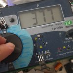
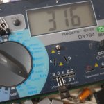
The gain you show is a little high so I'm wondering if these are genuine. They might be. What is the gain at Ic=5mA and 150mA - is that in spec.?
Yes- I use BC307's while I've got a few left. My new stock is BC557B, a replacement/equivalent. Mullard (Philips) manufactured some early/test BC237/BC307 but they went over to 547-557, and extended the range. Most of my BC237/BC307 were made by Motorola/ON Semi. The diagram should show BC557B.
There may be some "out there" which don't have a high ft - there was a similar range BD239 which are epitaxial base 3MHz-ish. If there are slow BD139's they're likely fakes. Measurement I've made on ST and ON Semi seem to suggest 100MHz+. Philips made the original devices, I believe, and they're over 100MHz as well. But Philips offloaded their semi manufacturing to NXP. The NXP datasheet shows typical gains around 150. I don't think Philips makes them now so anything purporting to be Philips may be fake or hopefully NOS.
The gain you show is a little high so I'm wondering if these are genuine. They might be. What is the gain at Ic=5mA and 150mA - is that in spec.?
Yes- I use BC307's while I've got a few left. My new stock is BC557B, a replacement/equivalent. Mullard (Philips) manufactured some early/test BC237/BC307 but they went over to 547-557, and extended the range. Most of my BC237/BC307 were made by Motorola/ON Semi. The diagram should show BC557B.
Last edited:

Currently it is an electro in my setup, though whether that is best is another question.
It will be biased in operation, and being large compared with the input resistance should have very little signal across it in use and not distort. My earlier distortion measurements were with that (and the 6.8mF output capacitor). Relatively low bias resistors (compared with JLH's 100k's) should mean leakage currents are less of an issue too.
It will be biased in operation, and being large compared with the input resistance should have very little signal across it in use and not distort. My earlier distortion measurements were with that (and the 6.8mF output capacitor). Relatively low bias resistors (compared with JLH's 100k's) should mean leakage currents are less of an issue too.
Last edited:
Continental Devices India cover a wide range of semiconductors including BD139 they also have a version of KSA3503 ( i.e.CSC3503). The range includes BC237-BC239 and BC307-BC309. Each of BC139 and BC557 is available over the counter at Jaycar in NZ and Australia and Altronics in Australia. One can order online however the only experience I have had with these is the process for overseas with Altronics has been a battle as they have had fraud issues with overseas buyers and it is not a simple case of entering credit card details for a cart.
The over the counter stocks include BF469 and BF470 used in older Television sets. For the BC 23X and 30X ranges mentioned above perhaps one would have to find a warehouse or other source in India.
Silicon Chip published an amplifier project a year or more ago in which BD139 was an option tried in a critical part of the circuit. I have a few of these in my part bin but I am away from home at present and also some BF469 and BF470 I am away from home and seem to remember these had CDI marking on them.
I have simulated another project where there were options to use BD139, 2SC3421 and KSC3503 as I have these to hand. I found no significant differences between these. I used Cordell's 2SC3503C for KSC3503. If there are any doubts about BD139 also using Cordell's model, then use of KSC3503 might resolve any lingering doubts
There were only two power amplifiers published by JLH that were offered without a passive (RC) input filter the present example of 1969 his first and another published in June -July1970 a Class AB variant which drew from the 1969 design.
All subsequent designs of his include passive RC input filters and this is quite normal practice with other designs.
In July 1969 he published a modular pre-amp which included an active steep filter which would limit the input signal to exclude frequencies beyond the audio spectrum. This pre-amp was intended for use with these two early designs and this has largely been forgotten along with the filter section.
The 1996 update of the circuit included an RC input filter 4R7 with 330pF by this time improvements had been made in source material so steep low pass filters of the 1950's and 60's with variable turn over frequencies with a selection of slopes as in the 1969 modular pre-amp were no longer necessary.
For a passive a 6dB/Octave filter has a turnover frequency of around 100kHz that would obviate the instability on a 10kHz square wave giving rise at a frequency of 285kHz.
In his book on Valve and Transistor Audio Amplifiers one of the requirements for an amplifier was that :-
"The phase linearity and electrical stability of the circuit, with any likely reactive load, should be adequate to ensure no significant alteration of the form of a transient or discontinuous waveform such as a fast square or rectangular wave, provided this would not constitute an output or input overload. There should be no ringing (superimposed spurious oscillation) and, ideally there should be no waveform overshoot under square wave testing, in which the signal should recover to the undistorted voltage level , +/- 0.5% within a settling time of 20uS."
A suitable low pass filter for this kit amplifier to avoid any hacking could be included in a preceding line stage in the feedback loop of an IC consisting of 4k7 Ohm with 330pF in parallel -such with an output buffer resistor at 220R and provision of +/- 15volt supply rails.
With regard to use of 60MHz unity gain output transistors there is some scope to increase the closed loop gain to a level where the suggested pre-amp could serve purely as a buffer.
It would have been possible to include a passive input filter and to increase the closed loop gain from 13 which is below average and to obviate the need for a buffer circuit.
A low order, low-pass input filter does seem like a sensible plan for any power amp. but it's location and design may need some consideration. Having the filter located in a preceding line stage preamp is likely to be restrictive and subject to misuse so perhaps you have some comments on how necessary this is likely to be when there are literally thousands of these DIY amplifiers working happily (apparently) with no more filtering than a bare volume control located between a line source and the basic JLH amplifier.
Assuming there really is something to be gained here without hidden penalties, how would you go about including the LPF in the JLH'69? Perhaps just insert a simple 3dB, RC LPF after the power amplifier's line input socket? e.g http://www.learningaboutelectronics.com/Articles/Low-pass-filter-calculator.php
Assuming there really is something to be gained here without hidden penalties, how would you go about including the LPF in the JLH'69? Perhaps just insert a simple 3dB, RC LPF after the power amplifier's line input socket? e.g http://www.learningaboutelectronics.com/Articles/Low-pass-filter-calculator.php
My comments relate to the amplifier kit sourced from China. I like the look of the assembled kit and some ingenuity of thinking has gone into this.
I think it is a pity that later changes to the circuitry made by JLH were not included and while some of this was covered in his book on Valve and Transistor Audio Amplifiers, the information in this which was available on publication in 1997, it seems this did not form part of whatever research.
According to JLH the dominant pole of the original amplifier was built in as the small signal transistors were faster than the 4MHz output transistors. Since and these rolled off at a tenth of the rate of the small signal devices, the outputs set the dominant pole, which ensured stability, and no compensation capacitor was necessary.
The received wisdom from where-ever is that this circuit would be improved by employing 30 MHz output devices and this view has become highly popular. Nonetheless some evidence has appeared in a Youtube video showing that some instability problems have been observed.
The suggested cure for this was to include a lead capacitor in parallel with the feedback resistor R11 in the first attachment. This would be a quick and easy excercise by soldering the capacitor to the pads of R11 under the pcb.
The first attachment shows JLH where uses capacitors in the feedback path - ie from the voltage gain stage to the inverting input. This strategy was also used by Nelson Pass whose first published amplifiers operated in Class A.
A possible problem with the lead capacitor in parallel with the feedback resistor is that capacitor impedance reduces with increasing frequency. With 30MHz or 60MHz output devices in lieu of 4MHz types, this increases the risk of possible transmission of out of phase signals, generated by a speaker load reaching the inverting input.
There are ways to reduce that possibility through an appropriate output stability network
i.e. use of resistor damped series inductors and Zobel networks. With a lead capacitor in parallel with the feedback resistor it is hard to see why that has not been included.
The approach taken by JLH with the 0.22R series output resistor and Zobel network could be added to the output of the board - see first attachment. This could be adopted externally in the housing for the kit from China.
The most recent JLH amplifier design a I am aware of, a MOSFET type added a damped inductor in series with the series
0. R22 resistor.
There was a follow up to the Class A circuit which addressed some stability questions from letters to the Editor of Wireless World due to layout issues. This is shown in the second attachment although there is no output choke. This circuit still relied on being matched with the modular pre-amp with steep low pass filters.
Attachments
mjona said "The first attachment shows JLH where uses capacitors in the feedback path - ie from the voltage gain stage to the inverting input. This strategy was also used by Nelson Pass whose first published amplifiers operated in Class A"
Which was also the approach I used in my suggested modifications for using 30MHz output devices, along with base resistors in the output transistors. These are necessary to roll off the gain at above 10MHz or there is a spike which may lead to instability. Simulations indicate an acceptable gain and phase margin, and testing so far has not uncovered any oscillations.
The problem with the proposed solution by JLH in the second attachment as I see it is that the 1nF capacitor and 100 ohm resistor across the base of the driver transistor cause a phase delay which slows the response - but as he also used 1nF where a 2.7k feedback resistor was used, the frequency compensation was rather top heavy, giving a bandwidth of about 60kHz?, so the 1nF and feedback work together, but not optimal for high performance audio.
This seems worse on the first circuit where 220pF was used with a 22k feedback resistor giving around 35kHz. Also with that circuit, the driver current is rather low (about 1.5mA) which is going to limit the slew rate into that 220pF capacitor, but as it is already bandwidth limited, that may not be the problem it may seem. I have not investigated any further.
I am a bit miffed on the last paragraph where you mention the 22k feedback resistor in the first circuit shown in post 9401.
Anyway the components in your bootstrap circuit are as per recommended for 8 Ohm loads in the original design. I built this in 1976 and it worked as expected. I did not measure the collector current of the driver transistor and this has been built by countless others over the years.
While bootstrap collector loads can operate at lowish levels 1.5 m.a. looks an odd result. I suggest you re-run your simulation with the resistor values JLH used in the original design.
While bootstrap circuits allow higher voltage outputs than constant current transistor loads in Lin style amplifiers, these are used solely to help amplify voltage.
In the present circuit there is a secondary function of driving the output devices in split phase which adds some complexity. In this the bootstrap circuit, positive in phase in drives the upper output transistor so it conducts more on opposite cycles when the lower output transistor conducts less.
At the point where the bootstrap capacitor connects to the output line, at point X in the original circuit diagram, this is shared a connection to the emitter of the input transistor and through a resistor of 2k7. The emitter also connects to an RC network to ground via 220 R in series with 250uF.
Between point X and ground there is an original a.c. impedance of 2920R. If the divider network resistor ratios are maintained but reduced in impedance that looks to have been an oversight.
The Ic current of the driver transistor is less than a tenth of that in simulations I have done albeit this is with circuits having a constant current on the driver transistor collector.
Last edited:
I wonder if we are discussing the same circuit. My reference to the 22k feedback resistor was to the first circuit you posted in #9430, showing a complementary ouptut stage using a Darlington pair driven from a driver pair making it effectively a triple CEF output stage. That was not the Class A design of this thread, but a Class AB. The bias for the output stage was derived across a 1k resistor, so for a bias voltage of about 1.5V that would have required about 1.5mA. Perhaps I should have made that clearer.
I think you are raising points about my circuit, in post 9402, In my proposed circuit for the Class A amplifier using high frequency transistors, I reduced the impedance of the feedback network. If that is what you are referring to, it was done to reduce distortion. It works in this way because the 220 ohms JLH used, added to the emitter impedance, generates something like 280 ohms effectively, giving a 3.6mA/V transconductance in the input stage. With 100 ohms, the overall impedance is reduced to 180 ohms giving a 5.6mA/V gain. I do not know why JLH chose 220 ohms but I suspect it may have been a stability concern. With more linear transistors in the output stage any second order distortion cancellation by the limited gain of a 220 ohm resistor in the original (if that was the intention or one of the design considerations) is no longer necessary and a higher OLG can be utilised.
That was not the final version of the circuit. In order to provide thermal compensation, which is more important for the modern transistors because they do not have the same gain roll off at the currents used in the JLH circuit, there are two options. JLH recommended shunting the current in the driver using a transistor on the base of the lower output transistor. That could be used but that option needs the bootstrapped resistor to be set to the lowest value needed for low gain transistors. The current can then be set in the PSU circuitry for any transistor pair.
Instead I chose, in my current revision, not the circuit in post 9402, to use a constant current source. Whenever a CCS is used there is a penalty of a small voltage offset which limits the output swing by a volt or so. That is a disadvantage in a Class A circuit when efficiency is impacted, but on the other hand, nearing clipping the output transistors will be exhibiting quasi saturation and having a falling gain, so distortion will be increasing when the differential across an output transistor is less than about 2V.
The CCS is used to control the current so that there is no need for an excess current, which would be the case for the shunt method if higher gain transistors are used, and the control transistor shunting the balance. This minimises the dissipation in the driver. Further, the CCS circuitry using a Class AB style bias stabiliser allows for adjusting the thermal compensation by setting the resistor ratios according to the degree of control required. In JLH's control circuitry, the compensation depended on the current setting. In my suggested circuit, you choose the resistor ratio according to the thermal resistance of the heatsink you plan to use.
If the small voltage drop across the CCS transistor ( no more than about 1V) is a problem, I would recommend using a voltage doubler on the PSU (bootstrapping the supply, if you like) and providing a regulator to set the voltage to it about 2V or so higher than the main supply. The resistors setting the bias to the CCS transistor will have to be adjusted accordingly.
A while back I bought a cheap already built board using TIP41 transistors, no schematic but it uses one pot for the current but none for voltage adjustment. I have the amp running off a laptop brick and with the current pot turned all the way up with 19V and 1.75A through the amp, the Dell brick is rated at 3.3A. At 200 Hz I get the following response into clipping. Normal?


Make sure the supply is what you think it is when its clipping.
What is the centre point voltage before the speaker coupling cap? It should be half the supply voltage approximately.
What load impedance is the amp driving in that image?
Edit... if the supply is only 19 volts then there is no point running it at 1.75 amps. Somewhere around .85A should be plenty.
The scope looks to be on 0.5 volt/div. I assume you are using a divider probe? What clean peak to peak swing can you get into an 8 ohm load?
Last edited:
The typical JLH circuit has to be tuned to the supply voltage and load impedance. The output is not the same under different loads. It is not flexible like a typical AB amplifier. And many "JLH" products are less than optimal. The simplicity of this amp appeals to beginners, but it takes someone who understands the fine points of the circuit operation to consistently get good results, although few experts are interested this topology in its classic form. I have extended it to THD of less than 0.01% in simulation of a class-AB variation. Class-A amps are like tube amps in that they are very forgiving of mistakes. I confess that I resent beginners who can afford expensive tools and materials that were out of reach to me at that age.
18V at terminals not 19V, I have some crappy test leads that did not like the current. 8.6V at the cap. The load impedance is 8 ohms. The scope probe is on X1.
Just for the heck of it I reversed the scope probe across the load. Low and behold a non-clipped sine wave across the full screen. I guess I missed a turn of the wire to the resistor, First time something like this happened to me, another nugget to put into my troubleshooting toolbox. Things are looking up. A little past 16V output. My god Mooly, you fixed it! Thank you very much.
Just for the heck of it I reversed the scope probe across the load. Low and behold a non-clipped sine wave across the full screen. I guess I missed a turn of the wire to the resistor, First time something like this happened to me, another nugget to put into my troubleshooting toolbox. Things are looking up. A little past 16V output. My god Mooly, you fixed it! Thank you very much.
I built a L'il Tiger amplifier in the 70's, pressed into guitar service for a buddy that did not have an amp (can not remember the preamp we used, still do have the Tiger downstairs still). It sounded great and my cousin was peaved as it got a great Marshall sound and his Fender Twin could not break into distortion. This stuck in my mind years latter when I read SS sucks for guitar. Which was odd as I built a small practice amp and when brought it to work one guy who took it home to try gushed over it and that it gave the sound he was looking for that he was not getting from his Fender Champs he bought chasing tone (which I occasionally ask what tone means).The typical JLH circuit has to be tuned to the supply voltage and load impedance. The output is not the same under different loads. It is not flexible like a typical AB amplifier. And many "JLH" products are less than optimal. The simplicity of this amp appeals to beginners, but it takes someone who understands the fine points of the circuit operation to consistently get good results, although few experts are interested this topology in its classic form. I have extended it to THD of less than 0.01% in simulation of a class-AB variation. Class-A amps are like tube amps in that they are very forgiving of mistakes. I confess that I resent beginners who can afford expensive tools and materials that were out of reach to me at that age.
Because of this I wanted to try a Class A amp designed from the time when the circuit was simpler and not relying on a ton of NFB. I do want to compare it to a tube amp yet, also a chip amp, the L'il Tiger and a PA amp that has a transformer output. Lots of time wasting, but heck I am retired.
I don't know why I can not quote you OldDIY, "Did you use insulating bushings for the BJT mounting screws?"
No I only managed to scrounge up a couple of mica insulators and scraped some heatsink compound off of a Led cob. I insulated the bolt head using a piece of circuit board and positioned the bolt through the center of the transistor and heatsink holes. Checked continuity between the heatsink and the tabs and tightened the bolts when there was no beep on the angry meter.
Guitar feeding back through a boost pedal and into the amp.

- Home
- Amplifiers
- Solid State
- JLH 10 Watt class A amplifier