Hi All, attached is a dual rail supply, CCS variant with differential input. Quick question, what is the recommended current for the differential input Q1 and Q2? Is the CCS Q3/Q13 adequate for this purpose?
To make the dc offset to zero, the differential input ccs is running as low as 0.79mA. Not sure if it is a good idea or not.
Please feel free to download and play with the circuit, any recommendation or modification are more than welcome!
If you look at conventional LTP circuits you will see lower values for R6 than 8.2k. If you reduce this to 1.5k then VR2 can be reduced to 240R.
In addition to getting ccs currents right, the transistor bias voltages have to be right
Also with LTP stages you will need a compensation capacitor to make your amplifier stable. Using Hood's method this would connect between Q6 collector and Q2 base and and the matching capacitor value will be relatively high in relation to Q6 collector current.
Ideally this capacitor should be made as low as possible, to keep the additonal loading on Q6 collector current down, and this is not helped by a value of 2.7k for R21.
Increasing the feedback network resistors allows proportionate reduction of the capacitor value needed. In your simulation I looked at 18k with R2 equal to 1k. Sometimes it helps to improve stability by increasing closed loop gain so give this a try.
Returning to the JLH design. I have always looked at it with disbelief. How can a bias system that crude work? It's a question worth looking at. First, it's class A so a variation of bias is fine as long as the heat is kept low enough. In class AB this would be a disaster.
Secondly as John Ellis has pointed out the design is far more complex than is obvious, types and quantities of distortion and why caused comes to mind. Complex in a good way. JLH other designs show this is his genius and not an inability to do a " me too " design.
To remind everybody this is my take on a Long Tail Pair JLH. It almost switches off the second transistor. If my guess is right you will win more than you give away doing this. I rather like the capacitor coupled version as it echos the Cavendish amplifier often shown as an early LTP. Doubtless a bit of work using Spice would be wise. Try to have more second harmonic distortion than third as the JLH. This LTP allows easier adjustment and more capacitor choices for AC/DC coupling. I don't doubt there will be errors here. My work always has them. That's way we build prototypes. This often comes from wanting to force an answer that I want to be true.
Happy New year all. Thanks to all for keeping this thread going. Sure it goes in circles. So does life.
BTW guys. I feel sure the use of fast outputs mostly is that they have Super Beta or aspects of that. My 2N3055 E ( ? ) have very good gain at 1 amp ( > 100 measured in a test rig ). I see something at 2.5 MHz which could be Ft. This was a mild ( 3dB ) oscillation which was cured by a small capacitor to BC337-40 collector base. 12 pF is my best thought on that. It is possible the cure is worse than the illness there, listen and measure. It was very marginal. A LTP version might be more in need of the capacitor.
I was asked what I thought about climate change recently. " Doing all the right things for maybe all the wrong reasons". The improved JLH clones also. We must always learn why something sounds better. If not we never move on to better things.
I was asked what I thought about climate change recently. " Doing all the right things for maybe all the wrong reasons". The improved JLH clones also. We must always learn why something sounds better. If not we never move on to better things.
HI Nigel on nap 140 schematics the speaker have two 0V....
0V means it's 0 volt with respect to power supply zero volt or ground. As the music plays that zero point will swing plus and minus. Up to +-50mV that would be considered fine for what should be zero with no music playing.
As you say, it's based on the NAP 140 but still is the JLH circuit.
My daughter gave me her old tablet. This is it. Old banana fingers can do it! Actually nearly all of my many computers are the kids cast offs.
Last edited:
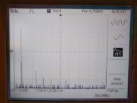
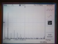
That's as far as I would dare go at +/-22V. 14 V rms is excellent. Did you get any small oscillation at 500kHz or above?
I have not seen any oscillations, at least for now.
Today I have repeated the oscilloscope testing for KTC3206 and 2SC2705.
The results are not exactly what I expected, especially for 2SC2705 which is 2SC3423 in the TO92 case. It seems that 2SD438 (sanyo) is the best, not just by oscilloscope but also by sound tests.
I still have to try 2SC2229 and again the TTC004B, and I hope I get some Y versions of C2705 and C2229 for testing.
Attachments
you tested this schema in real?
if so, what can you say about listening?
Not yet. Hope someone can do a sim.
Not yet. Hope someone can do a sim.
In a common emitter stage the gain Av = gm times the load in k Ohms where gm is about 40 per m.a. of collector current.
If the to be driven stages that follow the LTP have low impedance the outlook is not rosy.
In one of my simulations I could apply 21 dB of feedback at unity gain. At this point the phase shift is -100 degrees, giving 80 degrees margin and a gain margin of - 31.7dB.
I have not looked at a THD simulation since this is not a stand alone circuit.
Me also for other reasons. I will be moving house soon so find it difficult.
That gives me an idea. Maybe put together a mini workshop to use now and when at the new house.
Lets be clear. My LTP is to simplify setting up and analysis, I would guess 97% as good at a wild guess as the JLH 1969 design. My fear is that much is lost by doing that which I didn't see. In my circuit I have not dared asked how good the original circuit is . That could come later. Some will say LTP has a loss between second transistor and first. Yes, perhaps. It will have some time delay. An emitter follower driving a common base is not bad, that is a LTP. The original is common base with respect to feedback. Apart from that the JLH is a LTP with it's second transistor removed. The speaker output has plenty of current to drive the common base first transistor, often current rules out common base ( CB ). The compromise is there is a loss in the first feedback resistor that has to be adjusted for when CB. Thus the very low current the 8K2 sets. The next transistor ( driver splitter ) acts as a voltage clamp which is of great utility as well as doing it's obvious two jobs ( there are more in how it shares ). It is possible that the LTP for current alone might help the JLH69. Douglas Self usually talks about the Sugden design and says it's sharing of duties between power transistors gives very poor balance. The Sugden is remarkably primitive. It could be this same defect that is the magic of these designs. Big valve designs meet many Self ideals. To me they don't sound very good. Many SE valve designs with the Self defects sound fantasitic. The not very good valve designs sound heavy. This is not bandwidth as one design I built started to roll off at 7.5 kHz. It sounded open and bright!!! It had no loop feedback. With feedback it sounded like many other nothing special designs. Even 6dB which made it linear far after 20 kHz! It used a modern Vox AC 30 transformer of 500H! No wonder Vox sound good. 120H is excellent. This was measure the Williamson way using the heater transformer. It wasn't leakage inductance that caused the roll off, capacitance caused it.
The 1979 Hitachi MOSFET design used two LTP and current mirror and 47K tail resistor!!! This gives a double slew rate with near perfect sink and source equal current and forms a near perfect voltage clamp to LTP1( 2% balance typical, better if adjusted ). With only 7 active devices it gives 150 watts 4R and very little distortion up to 100 kHz. What it proves is don't believe all you read. The Hitachi should not work. It sounds wonderful even with transistors like MPSA42/92 that on paper fall way short of 2SA872A 2SD756C 2SB716C ( > 300 beta ). It has a diode also which the currenct mirror requires ( can be a transistor ). BUZ900/905 can be used.
The JLH 8K2 first transistor collector load into the driver splitter in mine and JLH sees a very low current. It must be pure transconductance I assume stage to stage. It is typical of the era. When class B I doubt it would be very good. In class A perhaps it's fine? That's a question no one asks as far as I know?
The only Naim amp I know well is NAP 250. It's harmonic structure is almost like the JLH which seems to be it's imbalanced LTP ( long tail pair ). It's slightly more of the third harmonic than JLH which might give the Naim fast sound? When amps have mostly second they sound slow and dark. When balanced the sound is just right. This is irrespective of speakers used. That being true I suspect the measurement is showing traits of feedback rather than being the sound of the device. If not magic is at work. In a way that is OK.
Here is a specualation that might be true. We mostly infer everything from the voltage waveforms into a near resistive load. Perhaps a low open loop gain amp with low open loop distortion shows the latter in the current domain? That is we can hear something of the open loop sound when the reactive load is driven? Seems it should be true. The sad truth is we measure the voltage domain to be sure all is OK. Long after we know it is we continue to measure? That's a bit like using too many brush strokes when painting. Worse is people who never measure, they have no idea if the sound is a good version if anothers designs. Measure and listen.
Lets be clear. My LTP is to simplify setting up and analysis, I would guess 97% as good at a wild guess as the JLH 1969 design.
The only Naim amp I know well is NAP 250. It's harmonic structure is almost like the JLH which seems to be it's imbalanced LTP ( long tail pair ). It's slightly more of the third harmonic than JLH which might give the Naim fast sound?
If the harmonic structure of a Class A amplifier is monotonic it does not help to use the Naim imbalanced LTP. This can be seen in simulations.
The difficulty with common emitter stages is when a current flows in the load the voltage at the transistor collector changes. This impacts on the width of the collector and base diffusion boundaries - reflecting the amount of capacitance between the collector and base. With planar transistors roughly this is inversely proportionate to the square root of the voltage applied to the collector.
At the same time common emitter stages invert the signal so the collector to base capacitance is amplified by the gain of the stage and this appears at the base input. I have already commented about the amount of current being a factor in the amplification process - so the Vas transistor is going to dump the largest capacitance in comparison to the paired common emitter stages comprising the LTP inputs and one of these has to drive the Vas with the dumped capacitance.
The loading of the LTP collectors is thus in a state of imbalance as far as factors of Miller capacitance effects are concerned. In the Naim circuit the collector load resistor has been increased in value so the voltage at the inverting input transistor is low in relation to that in it's partner and therefore more capacitance arises and the variation of this under dynamic conditions will be less. I see this as part of the design strategy - when the capacitance is high the width of the base layer diminishes - you might like to ponder over that aspect.
The gain of an LTP stage is roughly half of a singleton input a 50/50 ratio. If this is changed to 8.2/180 the balance is too lop-sided in terms of Miller capacitance and the loading on the inverting input will need more drive from the feedback signal. In my simulation the closed loop gain dropped by 19dB without touching the divider network values - I attribute this to the loading on the feedback signal.
Some Thoughts on Existing Equipment Upgrades
If anyone is interested in upgrading by replacing the output 2N3055E (epitaxial base) transistors, I can suggest 2N3716 as a simple 150W drop in option.
This like the original MJ480/481 transistors in the 1969 article is a 4MHz device and the current gain range is 50-150 as compared with 2N3055 20-70.
A search "buy 2N3716" will show who has this in stock and using these will keep you in the same league as the original.
When I looked a simulation of the 1996 version using MJL21194 for output and BD139 in the phase - split position, the emitter current for the latter was 12-60 m.a. whereas the datasheet gives approximate current gain of 85-95 over that range with quite some curvature in between. These figures refer to full power of 15W.
At lower power levels the current variation will be a lot less but the smaller this can be made along a curve the better it will get towards a straight line.
Hi Mjona, thanks for your comment, much appreciated!If you look at conventional LTP circuits you will see lower values for R6 than 8.2k. If you reduce this to 1.5k then VR2 can be reduced to 240R.
In addition to getting ccs currents right, the transistor bias voltages have to be right
Also with LTP stages you will need a compensation capacitor to make your amplifier stable. Using Hood's method this would connect between Q6 collector and Q2 base and and the matching capacitor value will be relatively high in relation to Q6 collector current.
Ideally this capacitor should be made as low as possible, to keep the additonal loading on Q6 collector current down, and this is not helped by a value of 2.7k for R21.
Increasing the feedback network resistors allows proportionate reduction of the capacitor value needed. In your simulation I looked at 18k with R2 equal to 1k. Sometimes it helps to improve stability by increasing closed loop gain so give this a try.
 I hope I get it right with the modified circuit. Seems that if I increase the feedback resistor R21 anything >4k, I can't get the dc offset >100mV. Any comment are welcome
 Attachments
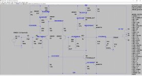
Hi Mjona, thanks for your comment, much appreciated!
Your circuit does not look too much different from simulations I have done for a lower power version LTP which I have not found the time to build.
The resistor values I gave in my last post were drawn from this so it is not hard to see where changes can be made. For the moment you should look at increasing the values in your nfb divider network - for a start try 22k and 1.8k and tune the emitter resistor value in the first CCS transistor.
I will look at doing some fuller simulations of your circuit in the next day or so. It is interesting that the Beta factor (BF) of 2N3716 is highest of the two power transistor .models
Hello Nigel, Mjona, Huggy and other participants to this thread.
I made a jlh1969 and still listen to it for about 4 years by now in parallel with my modified Hiraga 30w amp. Someone here asked about some listening impressions. Well here they are...
I used my Jlh with a Philips bc560c on input 2sc5171 as driver and a 2n3055+BD182 as outputs.
I listened to ST bd139-16 and bd140-16 on the Hiraga amp (1% matched) and wasnt so pleased because the 2sa1930/2sc5171 was clearer, more musical, and sounded more relaxed. I have tested 2 more types of drivers other than the famous bd139/140 or the 2sa/sc pair mentionned above but the 2sa/2sc was a clear winner. XRK and Hugh (AKSA) had confirmed that this pair is one of the most musical driver pair made novadays by Toshiba. I have some 2n1711 in the monkey box to test tomorrow and will report back, but i doubt that the 2N will beat the 2sc...
I made this amp from the monkey box with no pretentions whatsoever at the begining to test my speakers, but day by day i aded a small update and now it shines and sounds pretty darn good.
On the input i used a 0.68uf wima at 630v wich i tought was ok but bypassed it by a 0.33uf/250v wima mkp10; believe it or not these mkp10 caps if used at 630v version on the inputs instead of a 250v tend to sound muffled like it lackes hights... A friend of mine told me this thing first but didnt believe it till i tried. Now the sound is clear, with plenty of hights and a bit more bass.
At the begining i used a single 10000uF and thought it was ok, but after adding 0.5F/35v CrC cap bank from the Hiraga amp (just from curiosity) and seen the microdetails,details, bass, bass extension and dinamics, i realised that another 10000uF and a 0r22/6w wirewound inductive in CrC config was a minimall thing to do for only a single channel. So now i have a CrC (10000+0r22+10000) psu. Now the small humm that i have when putting the ear near the speaker has dissapeared (combined with a star ground) and have a rounder, deeper bass and cleaned overall sound.
In the past i used 1mm multifillar wire for the psu, now i use 2.5mm as in the Hiraga, wich made the amp a bit more responsive and relaxed with a bit more dinamics (interesting, this theory of Hiraga about cables is prety interesting). I'm planning to do the same with the outputs.
As for the outputs i tested today your theory guys, so i bypassed the 2k7 resistor with a 220pf styroflex cap and changed the outputs from 2n3055(IPRS Baneasa SA made) and the BD182 (who knows who made them) to MJ21194 (to204-a capsule, made in mexico, genuine ON part, ex Motorola) matched with the dmm and want to report that THIS IS THE REAL DEAL. What a clear sound i have right now, from the first turn on , from cold to warm, from min to max, everywhere.. The amp really changed, the bass is cleaner and more controlled, the mids are very very clear now and a bit more round, the hights are plenty now and clean, now you can really distinguish each and every instrument from complicated Mantovani and and his orchestra passages. Very recommended.
I listened to this amp to biases varying from 1A to 1.6A (had to add extra cooling to the originall heatsink as seen in the pics bellow to coup with the tremendous heat) and have to say that increasing the bias is a must, even if lowering the 27v psu voltage is the way to keep things cooler, because with each 100mA increment, the sound just gets clearer and clearer and more revealing, and relaxed. I highly recommend this.
I used a single 10000uf/35v rubycon bypassed by a 2200uf and 2.2uf and 0.1 uf in the past but now i use two industrial 3300 uf/63v/105c in parallel, and only a 33uf/180v extralytic cap to bypass. The bass is tighter than with the single 10000uf and more dinamic and cleaner.
Overall, now, if it werent to have the Hiraga amp, i will have made the 1969 jlh without a doubt, just for the customisation, the simplicity, the lack of need for matching and the warm sound.
Overall i like them both now, and SUBSCRIBE to what danw1milion and i spoke in private: you are right my friend, when increasing the bias, changing the outputs, this amp comes pretty close to the Le Classe A amp. I still have to try the split rail vers of the 69 amp.
Till then will test the 2n1711 and see..
Cheers
Sergiu
I made a jlh1969 and still listen to it for about 4 years by now in parallel with my modified Hiraga 30w amp. Someone here asked about some listening impressions. Well here they are...
I used my Jlh with a Philips bc560c on input 2sc5171 as driver and a 2n3055+BD182 as outputs.
I listened to ST bd139-16 and bd140-16 on the Hiraga amp (1% matched) and wasnt so pleased because the 2sa1930/2sc5171 was clearer, more musical, and sounded more relaxed. I have tested 2 more types of drivers other than the famous bd139/140 or the 2sa/sc pair mentionned above but the 2sa/2sc was a clear winner. XRK and Hugh (AKSA) had confirmed that this pair is one of the most musical driver pair made novadays by Toshiba. I have some 2n1711 in the monkey box to test tomorrow and will report back, but i doubt that the 2N will beat the 2sc...
I made this amp from the monkey box with no pretentions whatsoever at the begining to test my speakers, but day by day i aded a small update and now it shines and sounds pretty darn good.
On the input i used a 0.68uf wima at 630v wich i tought was ok but bypassed it by a 0.33uf/250v wima mkp10; believe it or not these mkp10 caps if used at 630v version on the inputs instead of a 250v tend to sound muffled like it lackes hights... A friend of mine told me this thing first but didnt believe it till i tried. Now the sound is clear, with plenty of hights and a bit more bass.
At the begining i used a single 10000uF and thought it was ok, but after adding 0.5F/35v CrC cap bank from the Hiraga amp (just from curiosity) and seen the microdetails,details, bass, bass extension and dinamics, i realised that another 10000uF and a 0r22/6w wirewound inductive in CrC config was a minimall thing to do for only a single channel. So now i have a CrC (10000+0r22+10000) psu. Now the small humm that i have when putting the ear near the speaker has dissapeared (combined with a star ground) and have a rounder, deeper bass and cleaned overall sound.
In the past i used 1mm multifillar wire for the psu, now i use 2.5mm as in the Hiraga, wich made the amp a bit more responsive and relaxed with a bit more dinamics (interesting, this theory of Hiraga about cables is prety interesting). I'm planning to do the same with the outputs.
As for the outputs i tested today your theory guys, so i bypassed the 2k7 resistor with a 220pf styroflex cap and changed the outputs from 2n3055(IPRS Baneasa SA made) and the BD182 (who knows who made them) to MJ21194 (to204-a capsule, made in mexico, genuine ON part, ex Motorola) matched with the dmm and want to report that THIS IS THE REAL DEAL. What a clear sound i have right now, from the first turn on , from cold to warm, from min to max, everywhere.. The amp really changed, the bass is cleaner and more controlled, the mids are very very clear now and a bit more round, the hights are plenty now and clean, now you can really distinguish each and every instrument from complicated Mantovani and and his orchestra passages. Very recommended.
I listened to this amp to biases varying from 1A to 1.6A (had to add extra cooling
to the originall heatsink as seen in the pics bellow to coup with the tremendous heat) and have to say that increasing the bias is a must, even if lowering the 27v psu voltage is the way to keep things cooler, because with each 100mA increment, the sound just gets clearer and clearer and more revealing, and relaxed. I highly recommend this.I used a single 10000uf/35v rubycon bypassed by a 2200uf and 2.2uf and 0.1 uf in the past but now i use two industrial 3300 uf/63v/105c in parallel, and only a 33uf/180v extralytic cap to bypass. The bass is tighter than with the single 10000uf and more dinamic and cleaner.
Overall, now, if it werent to have the Hiraga amp, i will have made the 1969 jlh without a doubt, just for the customisation, the simplicity, the lack of need for matching and the warm sound.
Overall i like them both now, and SUBSCRIBE to what danw1milion and i spoke in private: you are right my friend, when increasing the bias, changing the outputs, this amp comes pretty close to the Le Classe A amp. I still have to try the split rail vers of the 69 amp.
Till then will test the 2n1711 and see..
Cheers
Sergiu
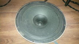
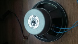
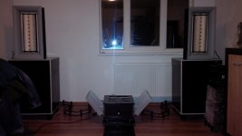
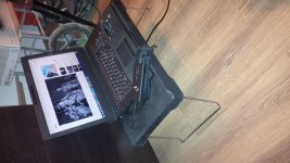
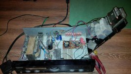
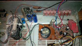
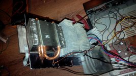
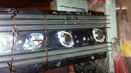
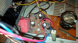
Here are some pics with my test equippment:
-speakers: SOLO full range (also called GAMMA) @8ohm and my diy rubanoide speakers+15 inch black cabinets;
-the jlh from the monkey box as seen with the diy radiator+ the modified Hiraga 30w (the satellite);
-the asus laptop+ emotiva big ego dac and diy input cables for the amps
No fancy smanchy no snake oil.
Attachments
-
 IMG_20181229_151526.jpg736 KB · Views: 504
 -
 IMG_20181229_151507.jpg479.9 KB · Views: 529
 -
 IMG_20181226_215953.jpg416.9 KB · Views: 541
 -
 IMG_20181226_220031.jpg755.7 KB · Views: 490
 -
 IMG_20181229_184959.jpg748.8 KB · Views: 187
 -
 IMG_20181229_185015.jpg693.2 KB · Views: 202
 -
 IMG_20181229_185121.jpg686 KB · Views: 195
 -
 IMG_20181229_185133.jpg698.2 KB · Views: 194
 -
 IMG_20181229_185105.jpg677.3 KB · Views: 212
Re Transistor Selection
With most variants of the JLH Class A circuit it is necessary to use a medium power transistor in the phase-split position. This is a consequence of the need to drive low current gain power transistors like 2N3055.
If these can be replaced by super beta types this opens the possibility of using some common small signal types like 2N5551 or for 2N3904 depending on the supply rail voltages ( to be safe with 2N3904 36volts or +/- 18).
If you look at the .models for these the VAF numbers are 667 and 400 high numbers like this indicate high Early voltage meaning these are less susceptible to base width modulation than devices like BD139 with a value of 99 and 2N1711 with 100.
As I have explained in an earlier post the capacitance between the collector and base transistor in a common emitter is inversely proportionate to the square root of the voltage applied to the collector. When a larger current is drawn through a load in the collector connection, the collector voltage will drop and the collector-to-base capacitance will increase.
The width of the collector region is proportional to the capacitance and when this increases the width of the base decreases. The outcome of this modulation process is a loss of current gain (and a recovery on the reverse cycle).
While I have put some emphasis on Early Effect (named after George Early) or VAF this has been investigated by Samuel Groner who came up with a rough calculation to consider the merit of a Vas transistor which is BF times VAF.
You also need to take the fT into consideration- some super beta power transistors might look attractive on Groner's calculation an fT of 30MHz is not good enough.
Also some transistors might have very good noise characteristics which might be the icing on the cake if you can get the mixture of that right.
One thing seems sure if you use the common garden transistors you are less likely to be buying the fake of an exotic transistor type.
Hello Nigel, Mjona, Huggy and other participants to this thread.
I made a jlh1969 and still listen to it for about 4 years by now in parallel with my modified Hiraga 30w amp. Someone here asked about some listening impressions. Well here they are...
I used my Jlh with a Philips bc560c on input 2sc5171 as driver and a 2n3055+BD182 as outputs.
I listened to ST bd139-16 and bd140-16 on the Hiraga amp (1% matched) and wasnt so pleased because the 2sa1930/2sc5171 was clearer, more musical, and sounded more relaxed. I have tested 2 more types of drivers other than the famous bd139/140 or the 2sa/sc pair mentionned above but the 2sa/2sc was a clear winner. XRK and Hugh (AKSA) had confirmed that this pair is one of the most musical driver pair made novadays by Toshiba. I have some 2n1711 in the monkey box to test tomorrow and will report back, but i doubt that the 2N will beat the 2sc...
With most variants of the JLH Class A circuit it is necessary to use a medium power transistor in the phase-split position. This is a consequence of the need to drive low current gain power transistors like 2N3055.
If these can be replaced by super beta types this opens the possibility of using some common small signal types like 2N5551 or for 2N3904 depending on the supply rail voltages ( to be safe with 2N3904 36volts or +/- 18).
If you look at the .models for these the VAF numbers are 667 and 400 high numbers like this indicate high Early voltage meaning these are less susceptible to base width modulation than devices like BD139 with a value of 99 and 2N1711 with 100.
As I have explained in an earlier post the capacitance between the collector and base transistor in a common emitter is inversely proportionate to the square root of the voltage applied to the collector. When a larger current is drawn through a load in the collector connection, the collector voltage will drop and the collector-to-base capacitance will increase.
The width of the collector region is proportional to the capacitance and when this increases the width of the base decreases. The outcome of this modulation process is a loss of current gain (and a recovery on the reverse cycle).
While I have put some emphasis on Early Effect (named after George Early) or VAF this has been investigated by Samuel Groner who came up with a rough calculation to consider the merit of a Vas transistor which is BF times VAF.
You also need to take the fT into consideration- some super beta power transistors might look attractive on Groner's calculation an fT of 30MHz is not good enough.
Also some transistors might have very good noise characteristics which might be the icing on the cake if you can get the mixture of that right.
One thing seems sure if you use the common garden transistors you are less likely to be buying the fake of an exotic transistor type.
- Home
- Amplifiers
- Solid State
- JLH 10 Watt class A amplifier