I would stick to lateral MOSFETs anyway.
There is a need for careful biasing.
If you know how to overcome the low transconductance, lateral is a winner (and this topo is not it). In JLH topology you sure need low (nonlinear) input capacitance for the splitter to drive, but if you look carefully there are even mosfets that have capacitance lower than laterals.
My electronics experience is firmly in the novice stage, but I do have a function generator if that helps debug.
This experience has also made me buy my first set of real premium cables ($100/m). Those ebay ultra premium cables ($30/m) were junk and were affected by emi from the power cable.
This experience has also made me buy my first set of real premium cables ($100/m). Those ebay ultra premium cables ($30/m) were junk and were affected by emi from the power cable.
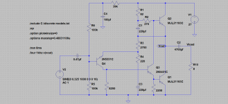
A true PNP version of the JLH should be configured as positive earth. Post your .asc file and I'll try it out.
Thanks Mooly, I'll upload them this evening when I get back from work.
Just regarding the input sine voltage - I usually run a .step until I find the clipping point then back the input voltage down a little before working on the circuit for distortion.
Is there a specific input voltage point that I should be setting - some kind of standard like 1/2 or 2/3 clipping?
Cheers
johnego,
the low transconductance of lateral MOSFETs cannot be overcome. It is a reason for good performance. Performance does not only depend on internal capacitances. Of course, you can go for a more efficient vertical MOSFET. What do you have in mind?
The disadvantage of phase splitter is that one of the output devices is driven by a weak base-emitter junction.
>>> the low transconductance of lateral MOSFETs cannot be overcome. It is a reason for good performance. Performance does not only depend on internal capacitances. Of course, you can go for a more efficient vertical MOSFET. What do you have in mind?
Paralleling output is obvious but expensive. Local feedback (compound pair) is another. Then there is the driving stage.
About low ciss mosfet, i have seen one or two types but i forgot the number and they are not current production items.
Paralleling output is obvious but expensive. Local feedback (compound pair) is another. Then there is the driving stage.
About low ciss mosfet, i have seen one or two types but i forgot the number and they are not current production items.
johnego,
The disadvantage of phase splitter is that one of the output devices is driven by a weak base-emitter junction.
The relationship between currents in a transistor is Ie= Ic +Ib in other words the charge carriers originate in the emitter a small fraction with be attracted to the base but the overwhelming majority will flow past the base to the collector.
The ratio of collector current to base current is called Beta or Ic/Ib for arguments sake say the result of this is 100.
The ratio of collector to emitter current is called Alpha or Ic/Ie.
From these two formulae and some algebra Alpha is equal to Beta/Beta+1 and Beta is equal to Alpha/1-Alpha.
Inserting the value of 100 into the elaborated equation for Alpha the result is 100/101 =99%
In other words the emitter current is greater than the collector current. For practical purposes the emitter and collector currents one would not split-hairs over the small difference.
That said if there is a disparity in the load presented by the stages driven by the collector and the emitter that could cause a slant on the balance such that the push-pull works notably better in one half cycle than in the other.
")
johnego,
you are getting lost.
mjona,
hfe (and Gm) is just a ratio expressing sensitivity.
The base-emitter junction exhibits a small force (amplitude) compared to the collector-emitter junction. This has little importance for DC biasing, but a great importance to signal transfer. Loosely speaking, the difference is qualitative. Charges are not equal as in numerical representations, but uniquely different with numerous ascribed characteristics.
Classical Physics has a low descriptive ability and is ambiguous and misleading. Maybe you should abandon it entirely.
Interesting.
Most of the .op commands were inherited from other's examples. The {freq} parameters etc were for running .step commands to find clipping etc.
I'd love to play with a corrected version if you don't mind uploading a copy?
Cheers
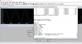
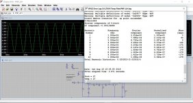
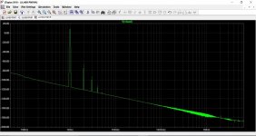
Here you go. Your sim I have altered to make all the caps massive (all 1 which is 1 Farad). This improves the visual result of the FFT and removes the slant that would otherwise appear. Input voltage set to give approx. 2.83vrms output which is 1 watt into 8 ohms.
Simulation time is set for 800ms and to start saving data from 600ms. That greatly improves the FFT result.
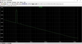
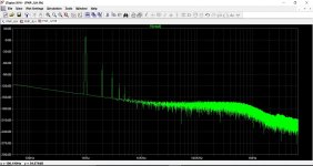
My original sim is just 'as is'. You can see the difference in the FFT due to leaving the caps at the design value and running the FFT for a shorter time (80ms and saving data from 60ms) and finally just running and saving for 8ms.
Attachments
[QUOT=N101N;5519953]johnego,
you are getting lost.
mjona,
hfe (and Gm) is just a ratio expressing sensitivity.
The base-emitter junction exhibits a small force (amplitude) compared to the collector-emitter junction. This has little importance for DC biasing, but a great importance to signal transfer. Loosely speaking, the difference is qualitative. Charges are not equal as in numerical representations, but uniquely different with numerous ascribed characteristics.
Classical Physics has a low descriptive ability and is ambiguous and misleading. Maybe you should abandon it entirely.[/QUOTE]
What I said was if with a transistor having a current gain of 100 the collector current in whatever units chosen would be 99% of the emitter current.
That leaves a difference of 1% in what ever units chosen for the base current.
The fact that the bias has to be arranged such that the base to emitter voltage results in a linear relationship between that and collector current is a given. For more on this see the extract of the BC546 spec sheet attached.
The fact that the 1% base current is small does not mean it is "weak" in a common emitter amplifier. The smaller this can be made the reduction in the range of operating current will make for a more linear result. This is possible using devices like BC546.
In an earlier post I gave a formula for Av the voltage gain of a common emitter stage. If you refer back to this an increase in Collector current will result in an increase in Av.
In a Class B system there will not be a great variation in collector current since the output stage involves a pair of drivers ahead of the power transistors and the foregoing points would be handy for that purpose.
This can still apply to the JLH input stage which also takes the form of a common emitter amplifier. However the split -phase transistor circuit will need to work a lot harder which rules out the use of a nice device like BC546 for this job.
Thus one has to be resigned to the facts the working current range of the selected device will be greater and it will not work quite as well as a BC546 or BC556 for the input transistor.
Attachments
The quality of JLH topology lies in comprising two single-ended stages. Single-ended stages do not disfavour any signal components, but set requirements for the power supply. A voltage regulator is a harmful option. Circuit simplicity is a fundamental condition in audio.
mjona,
you cannot make calculations for a dynamic process. Device type and bias current need to be determined intuitively, the current gain ratio is irrelevant here, loading is.
You cannot exercise tuition without knowing enough about what is involved. To do so is a matter of guesswork which is what simulations allow people to do.
Here we have a classic design where all the bits are assembled so there is a ready made starting point - but this does not tell you how or why it works.
There is something to learn from intuition from simple amplifiers but one can only go so far by skipping the 101 basics - e.g If someone has posted a circuit and another builds it and finds it does not work as it should - more-so where the circuit is complex.
Take note - from what I wrote in my last post there is an implication that the input impedance of the Class A output stage is lower than with a two element one like a Darlington and the split phase transistor is presented with a lower load so that part of the point you made about the influence of loading was already covered.
Re your other point it is not correct that the current gain is irrelevant since this is has a relationship with transconductance (gm) Volts in to Collector current out - where
Av=gm (roughly 40mS per ma) by RL load on the collector in k Ohms
A Siemen is equal to 1A per volt.
On device selection a figure of merit for signal stage transistors was given by Samuel Groner as the product of BF and VAF that is Beta factor and Early Voltage (check transistor .models).
Groner has written a number of interesting articles - I am giving one link from which the others can be accessed.
Analog Circuit Design · Samuel Groner · Resources · Power Amplifiers
In a later post you refer to single-ended operation. This refers to an active device drawing current from a voltage source through a single load. If the active device splits the load then the function is different since the two halves are driven in opposite phase.
Good morning guys!
I want to thank Mjona and Fredbloggstwo for the directions provided to me.
Unfortunately for the moment I have to postpone the experimentations, the wife wants to go on vacation and I have to settle. When I come back I propose to resume the thing and continue. For now, thanks and greetings.
Mleod
I want to thank Mjona and Fredbloggstwo for the directions provided to me.
Unfortunately for the moment I have to postpone the experimentations, the wife wants to go on vacation and I have to settle. When I come back I propose to resume the thing and continue. For now, thanks and greetings.
Mleod
- Home
- Amplifiers
- Solid State
- JLH 10 Watt class A amplifier