Argo,
No problem.
In my particular case if you look at Fig.1 JLH Class A for ESL57 in Geoff Moss's site you will see the feedback pick off point is connected between C4 and R7. That was before. Now I disconnect R7 from C4 and connect R7 very close to OUT.
In general when using feedback, it should follow this method to get the best location where to get feedback signals from IMHO.
Chris")
No problem.
In my particular case if you look at Fig.1 JLH Class A for ESL57 in Geoff Moss's site you will see the feedback pick off point is connected between C4 and R7. That was before. Now I disconnect R7 from C4 and connect R7 very close to OUT.
In general when using feedback, it should follow this method to get the best location where to get feedback signals from IMHO.
Chris
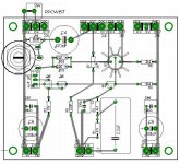
Feedback point
How do you do to go from the first 3rd of the board, where R7 is, to the third 3rd of the board where OUT is?
The reference I'm using for this question is fig 5 on:
http://www.gmweb.btinternet.co.uk/jlhesl.htm
Carlos
chris ma said:
if you look at Fig.1 JLH Class A for ESL57 in Geoff Moss's site you will see the feedback pick off point is connected between C4 and R7. That was before. Now I disconnect R7 from C4 and connect R7 very close to OUT.
In general when using feedback, it should follow this method to get the best location where to get feedback signals from IMHO.
Chris
How do you do to go from the first 3rd of the board, where R7 is, to the third 3rd of the board where OUT is?
The reference I'm using for this question is fig 5 on:
http://www.gmweb.btinternet.co.uk/jlhesl.htm
Carlos
Hi Carlos,
I removed the link between R9 and R7. Use a short length of hook up wire, solder one end onto the track close to the OUT. Press and bend the hook up wire and keep it as close to the board as possible and retrace the wire along the PCB track back to the track where LINK used to be and solder it onto the track thus connect the wire to R7. I did that in five minutes for both channels.
Chris
No no, C4 stay as is, sorry that I confused you, told you my english is bad
Let's use only Fig.5 as our reference ok, remove the LINK between R9 and R7, use a hook up wire to connect OUT and R7 by the C4 side( left side of R7nin Fig5). Thats all.
Reading back on what I posted for Argo I did make a mistake saying disconnect R7 from C4, no that is a mistake I meant C4 and R9 in Fig.1 and then jump over and bypass R9 and R11, reconnect it between R11 and OUT.
Sorry
Chris
Chris,
I see it now.
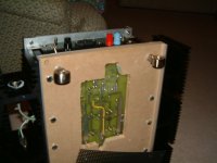
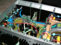
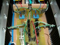
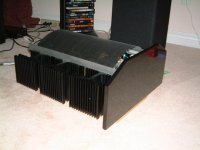
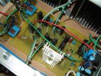
Here is my layout I am currently using if anybody is interested. Still can’t post any picture - no digital camera yet. Its on 8 x 10 cm Veroboard using component leads and solid 1mm tinned copper wire. Output transistors are connected with short 1mm solid wires as well. Signal ground (GND) is separated from power grounds (PE and PE’).
Argo

Ups.
There is an ERROR in the layout picture. Q6 emitter and collector shouldn’t be connected of course.
I see it now.
Here is my layout I am currently using if anybody is interested. Still can’t post any picture - no digital camera yet. Its on 8 x 10 cm Veroboard using component leads and solid 1mm tinned copper wire. Output transistors are connected with short 1mm solid wires as well. Signal ground (GND) is separated from power grounds (PE and PE’).
Argo
Ups.
There is an ERROR in the layout picture. Q6 emitter and collector shouldn’t be connected of course.
Attachments
Banned
Joined 2002
mrfeedback positive negative feedback feedback....
Chris, congrats on your new toy, and good on you for trying different physical arrangements, and more so for hearing them.
To further your findings, I have found the negative feedback signal pick off location to be very important.
IME, the summing point at the amplifier ouput point needs to be a "star earth" like arrangement to generate a correctly valid feedback signal, and that NFB signal shunt to ground components (R6, C3) need their own clean connection to central ground.
You have two causes for the change in sound that you now have from rearranging the NFB takeoff point, and they are changing or eliminating voltage jacking (due to resistance, inductance and leakage coupling) on the NFB line (physical pcb track), and that you have changed the conductor to a length of wire.
C4 will be passing relatively high current, and this will generate weirdo out of phase currents on the C4 to output point line.
However these voltage jacking effects and not always deleterious, and can be utilised to provide usefull local feedbacks.
For example R9, R11 and Out can be wired as R9-R11-Out, or R11-R9-Out, or seperated and following a star arrangement.
This can quite strongly affect output point and loading behaviour of the amplifier, and will most definately affect sonics.
I can tell you more if you you want to know.
Eric.
NFB
Thanks for the info Eric, love to learn more, wouldn't it be nicer for all newbies with a new thread regarding NFB take off point? be it point to point or pcbs.
BTW folks, I've forgotten to mention that I did try my best to ensure the hook up wire (length and size) and the exact points of soldering on the pcb track are identical on both channels.
Chris
- Home
- Amplifiers
- Solid State
- JLH 10 Watt class A amplifier