High-precision one
Well sort of too many similar pictures - ok, the last set for now")
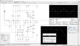
High-precision cascoded current mirrors, especially designed for audio (the ones I used in Lichtstark).
Note the level of distortion at 1KHz and at 500KHz Same slew rate.
This one is loaded with 10K resistor.
It's highly linear open loop.
3-rd picture - no global loop, loaded with 100KOhm, 64db gain, practically flat up to around 50KHz. THD=0.002%...0.004% all around the audio bandwidth.
Isn't it fun?
May be used as a cool front-end / line stage / head-amp core (with the buffer / OPS).
Paul (mcd99) has already simulated this kind of thing with jFETs (self-biased IPS arrangement). Lots of options
Well sort of too many similar pictures - ok, the last set for now
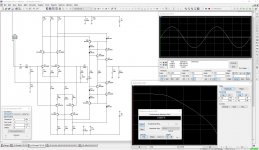
High-precision cascoded current mirrors, especially designed for audio (the ones I used in Lichtstark).
Note the level of distortion at 1KHz and at 500KHz
Same slew rate.This one is loaded with 10K resistor.
It's highly linear open loop.
3-rd picture - no global loop, loaded with 100KOhm, 64db gain, practically flat up to around 50KHz. THD=0.002%...0.004% all around the audio bandwidth.
Isn't it fun?
May be used as a cool front-end / line stage / head-amp core (with the buffer / OPS).
Paul (mcd99) has already simulated this kind of thing with jFETs (self-biased IPS arrangement). Lots of options
Attachments

Scott, was your idea similar to the "complementary OPA627" inspired circuit you posted in an earlier thread?
You mentioned there that it could be connected "a la AD797", perhaps it will stir up a few memories.
Best wishes
David
That was the circuit I used to demonstrate the tuning of offset and gain at the same time. There should be some pictures as I actually built it. The super bootstrapping reduces the effect of a bunch of device output impedance issues and non-linearities by making them common mode. This is how to get 5+ million gain out of a single stage.
Adding the positive feedback to eliminate crossover distortion would be a bit of work (I think). Another point is that once you do an output stage like a JE990 with some real quiescent current the trick does not buy you much. I was constrained to drive 600 Ohms at 7V rms on 500uA by the power budget.
What do you think?...
I think I will need more time to study all your ideas.
My own ideas are not quite fully developed and I hesitate to post them because my perspective seems a bit different to Scott's and it's awkward to debate with the person who came up with the circuit in the first place
But I hope it's a "cup half full / half empty" issue, a matter of viewpoint and not that I am incorrect.
Anyway, I see 2 aspects of distortion reduction in the AD797.
One is the driven current mirror, to provide enormous loop gain simply.
AFAIK this is a distinctive AD797 feature and I would like to incorporate it in my own circuit.
Second is the distortion "neutralization" capacitor.
I see both of these as essentially embedded +ve feedback loops and I consider this the fundamental reason for the superior performance of the AD797 .
Positive feedback scares many people but theory implies that a combination of +ve and -ve feedback loops can beat the performance of -ve feedback alone.
So what really interests me is this combined feedback structure.
I see the AD797 as a rare practical implementation of the idea, and an excellent place to start, I am not locked in to a slavish copy, the trade-offs are different for an audio power amplifier.
I hope that none of the above contradicts Scott's explanation of his own amp
I understand he initially disputed the feedback view of distortion neutralization but believe he may now see it as a useful.
Also, it recently hit me that that the distinction between +ve and -ve feedback is a false dichotomy anyway, on the complex plane it all blends seamlessly.
So I think this minor epiphany, when you realize what the maths actually means, unifies the different view points.
Best wishes
David
I originally used the analogy of neutralization of input capacitance with a synthesized negative capacitance. If you play around with different ways of looking at it you can even see the behavior of a gyrator. IMO some confusion lies around the fact that the bootstrapping is acting at the same time and the extra cap only "sees" the voltage across the output stage which is alway very small and it never sees any gain. There is not effectively a small amplifier inside the main loop feeding around the output Vbe's like some other error correction schemes (CFP?). If you examine the behavior vs. frequency while tuning that cap (especially the output impedance) it still looks like a vector null akin to a twin-tee network. So if calling it a small positive feedback works it's OK by me.
I used CFP's BTW in an ADSL driver (pain to get stable) that was a record for performance vs quiescent current. The output was biased at 250uA for 400mA peak current.
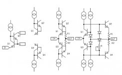
Here's another one, Barry Blesser published the "super transistor' on the far left decades ago. Imagine a time when a two transistor circuit was acceptable in the IEEE journal. I took a logical progression to the right for an error corrected output stage, a tiny CFA inside the loop.
Attachments
~= Pass "non-switching" Active bias circuit for operating push-pull amplifiers in class A mode with the drive moved
Good to see so many Gurus here 
I believed we discuss a-la AD797 arrangements mainly having the front-end / line stage applications in mind - in this case we can keep the output buffer in class A without bothering to minimize the crossover artifacts, IMHO.
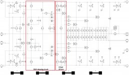
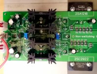
If we touch non-switching AB output stages as well - I'd like to share the work I did about a year ago - a bias clamping mechanism (a-la Technics non-switching), working especially well with CCSed driver stage.
Important points for the best results - the diodes (D1-D4) must be fast enough, the clamping voltage reference (spreader) must be temperature-compensated (places on the main heatsink).
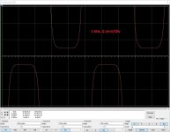
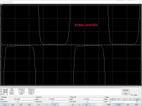
Diagrams illustrate the OPS emitter currents (measured as voltage drop on emitter resistors) at 1KHz and 20KHz (V/Div scales are different).
At 20KHz certain minor dynamic bias sagging is visible, however it does not degrade the performance.
Some people are concerned that the bias clamping mechanism is a "switching" one by its nature - not really, at the right currents through the diodes, the bias is picked-up smoothly - you can see the rounded corners.
Minimal dynamic bias shown is about optimal - at this level crossover residuals are just masked by noise. Moving it up or down from this level will result in distortion increase.
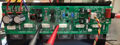
Pictures show the fragment of the early prototype board, as well as what it looks like nowadays (allowing interchangeable front-ends - very good layout work by Jeff Wilhelm).
Cheers,
Valery
I believed we discuss a-la AD797 arrangements mainly having the front-end / line stage applications in mind - in this case we can keep the output buffer in class A without bothering to minimize the crossover artifacts, IMHO.
If we touch non-switching AB output stages as well - I'd like to share the work I did about a year ago - a bias clamping mechanism (a-la Technics non-switching), working especially well with CCSed driver stage.
Important points for the best results - the diodes (D1-D4) must be fast enough, the clamping voltage reference (spreader) must be temperature-compensated (places on the main heatsink).
Diagrams illustrate the OPS emitter currents (measured as voltage drop on emitter resistors) at 1KHz and 20KHz (V/Div scales are different).
At 20KHz certain minor dynamic bias sagging is visible, however it does not degrade the performance.
Some people are concerned that the bias clamping mechanism is a "switching" one by its nature - not really, at the right currents through the diodes, the bias is picked-up smoothly - you can see the rounded corners.
Minimal dynamic bias shown is about optimal - at this level crossover residuals are just masked by noise. Moving it up or down from this level will result in distortion increase.
Pictures show the fragment of the early prototype board, as well as what it looks like nowadays (allowing interchangeable front-ends - very good layout work by Jeff Wilhelm).
Cheers,
Valery
Attachments
~= Pass "non-switching" Active bias circuit for operating push-pull amplifiers in class A mode with the drive moved
Well you see the PTO has their own meaning of obvious. Blesser was long before that.
Last edited:
- Status
- This old topic is closed. If you want to reopen this topic, contact a moderator using the "Report Post" button.
- Home
- Amplifiers
- Solid State
- Fully complementary AD797?