Hello All,
I have recently been working on making some improvements to a small power amplifier I made back about a year ago (see result of that thread here). Since then, I have done a few iterations on the design, both to increase the output power and to add current regulation to the biasing to reduce any mains hum.
My question is, how can I improve this design? I am still fairly new to all this, so I'm always looking for ways to improve my designs or catch mistakes. I have not done any physical testing of this circuit, so I do not yet know if it will actually work.
A few notes on this design:
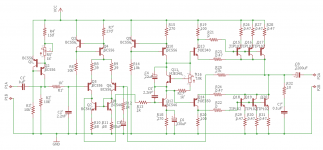
1. The design is meant to be powered nominally from a single-ended 48V supply, but the bias current adjustment at R5 should allow for a power supply range of about 36-65V. The speaker impedance is 8 Ohms nominal, but is designed to also work down to a 4 Ohm speaker impedance.
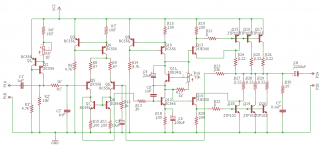
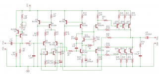
2. In an effort to increase the efficiency, I have opted to use TIP102/107 Darlington pair transistors instead of the IRF540N/9540N MOSFETs as with my previous design, and I made some changes to the output stage. (Please note that the Eagle Schematic does not show the transistors as being Darlington pairs, but that is mainly because I am just using a generic TO-220 transistor package for when I do the PCB layout.)
3. The three pairs of TIP102/107s may not all be populated on the final board depending on the supply voltage, speaker impedance, and heatsinking configuration. I could probably get by with one or two pairs, but I also plan to experiment with rearranging the feedback to try ganging two together in a differential configuration, so I'm planning to play it safe on the thermal side.
4. The adjustment trimmer on Q11 should allow for use with either darlington BJTs or MOSFETs interchangeably, in which case I would populate R21 and R22 with 220 Ohm resistors or similar (I'm open to suggestions for the exact value on that") ). Q11 will also be mounted on the heatsink with the power stage.
). Q11 will also be mounted on the heatsink with the power stage.
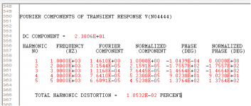
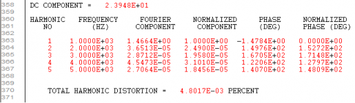
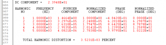
5. THD at 1kHz and 1Vrms output was calculated at approx. 0.01% for the 1st 5 harmonics. THD at 10Vrms was calculated at closer to 0.006%. What is a good frequency and or output level for calculating THD? I couldn't seem to find much info on any kind of standard values for testing THD.
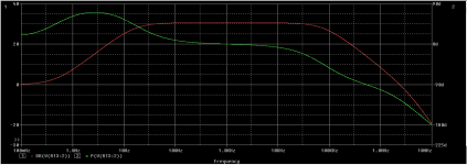
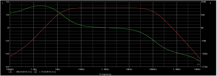
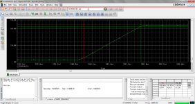
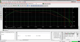
6. Phase margin is approximately 56.5 degrees. Gain margin is 19.75 dB. I have included two bode plots, one including the input filter and one that bypasses it for when I calculated the phase/gain margins.
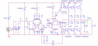
7. I originally was going to simulate for the current regulating transistors in the PSpice model, but I was exceeding the allowed limit for transistors in Orcad, so unfortunately I had to simplify the schematic with ideal current sources instead. All component designations (e.g. R10, Q3, etc.) should be based on the Eagle Schematic.
My plan is to try this circuit out on a breadboard, then eventually draft up a PCB layout of the final design. I have made a lot of changes back and forth between the simulation and schematic, but they should hopefully match up for all of the values shown.
Please let me know your thoughts and any corrections and/or improvements.
I have recently been working on making some improvements to a small power amplifier I made back about a year ago (see result of that thread here). Since then, I have done a few iterations on the design, both to increase the output power and to add current regulation to the biasing to reduce any mains hum.
My question is, how can I improve this design? I am still fairly new to all this, so I'm always looking for ways to improve my designs or catch mistakes. I have not done any physical testing of this circuit, so I do not yet know if it will actually work.
A few notes on this design:
1. The design is meant to be powered nominally from a single-ended 48V supply, but the bias current adjustment at R5 should allow for a power supply range of about 36-65V. The speaker impedance is 8 Ohms nominal, but is designed to also work down to a 4 Ohm speaker impedance.
2. In an effort to increase the efficiency, I have opted to use TIP102/107 Darlington pair transistors instead of the IRF540N/9540N MOSFETs as with my previous design, and I made some changes to the output stage. (Please note that the Eagle Schematic does not show the transistors as being Darlington pairs, but that is mainly because I am just using a generic TO-220 transistor package for when I do the PCB layout.)
3. The three pairs of TIP102/107s may not all be populated on the final board depending on the supply voltage, speaker impedance, and heatsinking configuration. I could probably get by with one or two pairs, but I also plan to experiment with rearranging the feedback to try ganging two together in a differential configuration, so I'm planning to play it safe on the thermal side.
4. The adjustment trimmer on Q11 should allow for use with either darlington BJTs or MOSFETs interchangeably, in which case I would populate R21 and R22 with 220 Ohm resistors or similar (I'm open to suggestions for the exact value on that
). Q11 will also be mounted on the heatsink with the power stage.5. THD at 1kHz and 1Vrms output was calculated at approx. 0.01% for the 1st 5 harmonics. THD at 10Vrms was calculated at closer to 0.006%. What is a good frequency and or output level for calculating THD? I couldn't seem to find much info on any kind of standard values for testing THD.
6. Phase margin is approximately 56.5 degrees. Gain margin is 19.75 dB. I have included two bode plots, one including the input filter and one that bypasses it for when I calculated the phase/gain margins.
7. I originally was going to simulate for the current regulating transistors in the PSpice model, but I was exceeding the allowed limit for transistors in Orcad, so unfortunately I had to simplify the schematic with ideal current sources instead. All component designations (e.g. R10, Q3, etc.) should be based on the Eagle Schematic.
My plan is to try this circuit out on a breadboard, then eventually draft up a PCB layout of the final design. I have made a lot of changes back and forth between the simulation and schematic, but they should hopefully match up for all of the values shown.
Please let me know your thoughts and any corrections and/or improvements.
Attachments
How can I improve this design?
The negative feedback loop capacitor should be much larger, at least 100uF or more, instead of 10uF.
Last edited:
- Many people, including the designer of the Threshold S300 (Nelson Pass), like to short together the collectors when using several Sziklai pairs in parallel. See attached schematic. In post #1 figure 2, that would be the collectors of Q15-Q16-Q17 and also the collectors of Q18-Q19-Q20.
- The AC gain is awfully high: (R25+R26)/R26 = 34X. Power amps usually have an AC gain more like 20X.
- I'd be more comfortable if R24 was an adjustable trimmer pot instead of a fixed resistor, so I could dial in the desired bias current within half a milliamp.
- I'd be tempted to try out the advice Douglas Self hammers again and again in his power amp book: be sure to insert an emitter follower between the input stage (collector of Q2) and the voltage amplification stage (base of Q3). This lightens the load driven by the input stage, and helps the compensation capacitor (C5) work its pole-splitting magic.
Attachments
I'd have my doubts about the output stage design. Move the 0.22s to the Darlingtons' emitters instead, give Q12/13 some dedicated emitter resistors (EDIT: like what Mark Johnson shows above), and play with R23/R24 to obtain a decent bias point (the high and dominant 3rd distortion indicates things are almost certainly underbiased).
Rayma, Thanks for the suggestion. I calculated 10uF to come out to a low-frequency cutoff of around 16Hz (1/(2*PI*1000*1E-5)=15.92). What is the benefit of making it higher?
Mark,
Hmm, that seems like a good idea. Looking at my circuit again, it probably makes sense to put the 0.22 Ohm resistors on the emitters of the output transistors instead of the collectors.
Really? I recall being told last time around that the "de facto" standard was around 29dB? See here.
R23/R24 on the Pspice schematic is meant as a 10k, 10-turn trimmer and a 1k resistor in series, as shown on the Eagle schematic I recommend going by the numbering on the Eagle Schematic, since it actually has all of the components shown. (I was too lazy to make the designations match lol).
Definitely doable. I'll mess around with it.
Thanks for the advice!
I calculated 10uF to come out to a low-frequency cutoff of around 16Hz
(1/(2*PI*1000*1E-5)=15.92). What is the benefit of making it higher?
This capacitor is part of the negative feedback loop, and is critical. To minimize distortion,
it should have low enough impedance that there is virtually no signal voltage across it.
Also, the input HP filter has the same time constant, and these poles should be staggered.
Since the input filter is set at 16Hz, all other circuit poles should be lower in frequency by several octaves.
This goes for the emitter bypass capacitor on the VA as well, it should be around 1000uF, rather than 100uF.
Last edited:
16Hz 3dB
Single roll-off.
The effect of double roll-off:
Hz single double
2.0 -16.5 -32.9
2.3 -15.5 -31.0
2.6 -14.5 -29.0
3.0 -13.5 -27.0
3.5 -12.5 -25.0
4.0 -11.5 -23.0
4.6 -10.5 -21.0
5.3 -9.5 -19.0
6.1 -8.5 -17.0
7.0 -7.6 -15.1
8.0 -6.6 -13.3
9.2 -5.8 -11.5
10.6 -4.9 -9.9
12.1 -4.2 -8.4
13.9 -3.5 -7.0
16.0 -2.9 -5.8
18.4 -2.3 -4.7
21.1 -1.9 -3.8
24.3 -1.5 -3.0
27.9 -1.2 -2.4
32.0 -0.9 -1.9
36.8 -0.7 -1.4
42.2 -0.6 -1.1
48.5 -0.4 -0.9
55.7 -0.3 -0.7
64.0 -0.3 -0.5
73.5 -0.2 -0.4
84.4 -0.1 -0.3
97.0 -0.1 -0.2
3dB is actually closer to 24Hz and 1dB about 45Hz
I go with rayma at 10 X lower.
Last edited:
All,
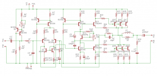
I have made some of the recommended changes to the design. Please see the updated schematic.
changes are:
-changed 0.22 Ohm resistors to be at the emitters instead of the collectors, added additional 0.22 Ohm resistors to the emitters of Q13 and Q14.
-changed C3 to 100uF, C4 to 47uF, and C6 to 1000uF.
-changed R25 to 27k instead of 33k, for a gain of 27.
simulations show 3dB cutoffs at 16.5Hz and 76kHz with the input filter included. THD is still around 0.01% at 1VRMs out for about 100mA bias current per pair. phase/gain margins are 56.3 degrees and 19.4dB, respectively.
I tried adding an emitter follower between Q7 and Q12, but it actually made the circuit unstable in simulation. The worst-case current gain of the power stage should be around 6000 for 1 pair of TIP10Xs, and around 30000 for 3 pairs, so the amplification stage only runs at a bias current of 7mA, and even that is probably more than I need. Q12 should be pretty sensitive, so is the emitter follower necessary?
I also tried changing R25 to 22k for a gain closer to what Mark recommended, but the simulation didn't really show any difference in stability or distortion, so I would prefer to keep the slightly higher gain.
If I were to use a capacitor with a lower voltage rating than the supply voltage for C6, would it make sense to add a zener across it? on paper, the voltage across C6 will never be that high.
Attachments
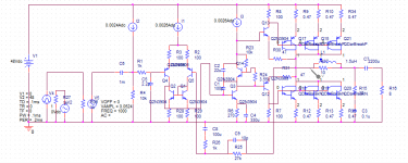
All,
In light of my own comment above about the bias current on Q12, I have changed the circuit to use a 2.6mA bias current instead of a 7mA bias current.
This allows me to increase R3, R6, and R14 to 10k (the original 4.7k resistors would have been probably 1W resistors for safety, so hopefully now I can dial that back to 1/2W 10k resistors). R7, R15, and R18 have been changed to 270 Ohms, C4 has been changed back to 22uF, and C6 has been changed to 330uF (all of these values should have a low-frequency cutoff below 2 Hz).
I have also changed R23/R24 and R26-R31 to 0.47 Ohms, if only for the reason that the current biasing trimmer will be really sensitive even if I use a 10-turn trimmer. I may add another resistor to Q11 just to narrow the range a bit. C2 and C5 have been increased to 2.2nF to improve phase margins.
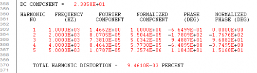
THD=0.005% for 100mA/pair, PM/GM = 66degrees/14.5dB. 3dB cutoffs with the input filter are around 16.5Hz and 32.5kHz.
Let me know if you have any additional corrections or thoughts.
In light of my own comment above about the bias current on Q12, I have changed the circuit to use a 2.6mA bias current instead of a 7mA bias current.
This allows me to increase R3, R6, and R14 to 10k (the original 4.7k resistors would have been probably 1W resistors for safety, so hopefully now I can dial that back to 1/2W 10k resistors). R7, R15, and R18 have been changed to 270 Ohms, C4 has been changed back to 22uF, and C6 has been changed to 330uF (all of these values should have a low-frequency cutoff below 2 Hz).
I have also changed R23/R24 and R26-R31 to 0.47 Ohms, if only for the reason that the current biasing trimmer will be really sensitive even if I use a 10-turn trimmer. I may add another resistor to Q11 just to narrow the range a bit. C2 and C5 have been increased to 2.2nF to improve phase margins.
THD=0.005% for 100mA/pair, PM/GM = 66degrees/14.5dB. 3dB cutoffs with the input filter are around 16.5Hz and 32.5kHz.
Let me know if you have any additional corrections or thoughts.
Attachments
Last edited:
It's kinda getting there.
A 2n2 compensation cap (C5) is extremely high, normal values tend to be around 47-100 pF, maybe 150 pF on a seriously old/slow design. You're not even in the ballpark. With some bad luck your output stage is a hopeless mess of poles. Slew rate can't be too high in any case, what's it like? A 2n2 C2 also is quite heavy.
R23/24 strike me as way low and could let driver currents become dangerously high, try something more like 10-47 ohms.
CFP output stages often benefit from some Miller capacitance on the pnp driver, so try something 100pF-ish on Q14.
I'm not sure whether you really need R13, but a few hundred ohms (or even R || RC) in the bases of Q13 and Q14 seem worth a shot.
Not sure how fast Q11 would still be at only 2.6 mA, but you've got a bypass cap at least. The bias circuit does not strike me as failsafe should the pot wiper ever go open. Try 1k || 10k pot in the lower leg and a resistor in the upper leg that gives your a decent bias adjustment range (start with 820-910R or so).
Speaking of bias, what sort of current does each pair of Darlingtons get? I would hope for 30-50 mA, and try up to 100 with emitter resistors down to 0.22.
You're also missing an output series LR network (~1.5 µH || 10R).
Using a current source for input bias seems overly fancy, anything wrong with a 10k / 10k||22µ divider followed by a 22-100k? Once you've got compensation sorted, I'd also consider running the inputs a bit less hot, 500 nA at 100-220 ohms of degeneration should also do just fine while giving less potential for input impedance distortion.
Wait, does distortion really say 4.8e-3 %, i.e. 0.00048%? That's unloaded though, isn't it? And at little over 1 Vrms output, too, apparently.
Last edited:
I go with rayma at 10 X lower.
I've always found that a dominant single LF pole sounds clearly better, with deeper,
more detailed, and more natural sounding bass.
If I were to use a capacitor with a lower voltage rating than the supply voltage for C6,
would it make sense to add a zener across it?
Skip the Zener, but it's best to make the C6 voltage rating the same as the supply,
to avoid cascading failures.
Last edited:
It's kinda getting there.
A 2n2 compensation cap (C5) is extremely high, normal values tend to be around 47-100 pF, maybe 150 pF on a seriously old/slow design. You're not even in the ballpark. With some bad luck your output stage is a hopeless mess of poles. Slew rate can't be too high in any case, what's it like? A 2n2 C2 also is quite heavy.
R23/24 strike me as way low and could let driver currents become dangerously high, try something more like 10-47 ohms.
CFP output stages often benefit from some Miller capacitance on the pnp driver, so try something 100pF-ish on Q14.
I'm not sure whether you really need R13, but a few hundred ohms (or even R || RC) in the bases of Q13 and Q14 seem worth a shot.
Not sure how fast Q11 would still be at only 2.6 mA, but you've got a bypass cap at least. The bias circuit does not strike me as failsafe should the pot wiper ever go open. Try 1k || 10k pot in the lower leg and a resistor in the upper leg that gives your a decent bias adjustment range (start with 820-910R or so).
Speaking of bias, what sort of current does each pair of Darlingtons get? I would hope for 30-50 mA, and try up to 100 with emitter resistors down to 0.22.
You're also missing an output series LR network (~1.5 µH || 10R).
Using a current source for input bias seems overly fancy, anything wrong with a 10k / 10k||22µ divider followed by a 22-100k? Once you've got compensation sorted, I'd also consider running the inputs a bit less hot, 500 nA at 100-220 ohms of degeneration should also do just fine while giving less potential for input impedance distortion.
Wait, does distortion really say 4.8e-3 %, i.e. 0.00048%? That's unloaded though, isn't it? And at little over 1 Vrms output, too, apparently.
Hmm, all very valid stuff.
First off, wouldn't 4.8E-3 be 0.0048%, not 0.00048%? That's with an 8 Ohm load, as per the Pspice schematic in the first post (I didn't want to upload both schematics each time just to avoid confusion because the component designations don't match up). I'm not sure what output amplitude would be best for testing. I also tried 10Vrms out, which actually results in lower distortion numbers, presumably due to the crossover distortion making up a lower percentage of the total waveform.
The current regulated input biasing may be a bit excessive, but I have intentionally done this so that this design can be run off of noisy or unregulated supplies with minimal mains hum/noise.
The Darlingtons have been simulated to roughly 100mA/pair bias current, but I suppose I could bias it to whatever I please on the real thing.
I calculated the slew rate to be about 0.6V/us. I'm beginning to see why that would be a problem. Lowering C5 to 100pF increases the slew rate to about 13V/us, but the stability margin drops to about 8 degrees/3.6dB. how would I better stabilize for this while still maintaining a fast response time?
I'll work on updating the rest of the circuit as per your suggestions.
Last edited:
Skip the Zener, but it's best to make the C6 voltage rating the same as the supply,
to avoid cascading failures.
Initially, I thought "that would take up a lot of board room", but then I saw on the PCB layout how big the 2200uF cap will be
Oh well.Okay, I was able to implement and simulate for most of the suggested changes. Hopefully things are starting to look a bit better, and this is definitely educational for me.
-C5 has been changed to 100pF, I added a 10pF capacitor (C9) across R26 to help improve stability a bit.
-R23/R24 have been changed to 47 Ohms. R8/R9 and R10/R11 have been changed to 100 Ohms. R13 has been removed.
-R16/R17 have been re-worked so that the quiescent current will not spike up if the wiper goes open circuit.
-A 1.5uH inductor and 10 Ohm series resistor has been added at the output (L1 and R33)
The slew rate now simulates to be about 23 V/uS. THD is around 0.0035%. PM/GM are around 80 degrees/ 12.5dB.
I tried lowering the current on the differential stage, but it seemed to have a negative impact on slew rate. Do you think that there will be a significant improvement is THD if I were to lower the quiescent current in the differential stage and/or increase the current in the amplification stage? Maybe I would need to lower the current on the differential stage and add an emitter follower between Q7 and Q12 as was suggested previously by Mark Johnson?
I will also mess around with adding a Miller capacitor to Q14.
Attachments
Last edited:
All,
I have run a bunch more simulations trying to lower the quiescent current of the differential stage, but it seems that doing so would directly limit the slew rate of the amplifier. What would folks consider to be an acceptable slew rate? By my calculations, If I were to use this at the full 65V supply voltage, I would need a slew rate of at least 8.2V/us for a full 65V swing at 20kHz (2*PI*20,000*65/1,000,000=8.164). I have also tried adding in an emitter follower between the differential and amplification stage, but this seems to make the system unstable.
I also tried adding a 100pF Miller capacitor across Q14, but it didn't seem to have much effect aside from lowering the stability margin. Is this supposed to improve distortion, response time, or something else?
Unless folks have additional thoughts on how I might implement these suggestions correctly or have other improvements to suggest, I might move forward with making a prototype of this.
I think Bob Cordell's advice in section 6.1 of his book, is conservative and appropriate. He recommends that you have sufficient slew rate to support a full-power sinewave output at 50 kHz. Using calculus to take the derivative,
For a different amplifier running with (+65V, 0.0V) rails, Cordell recommends > 10.0 Volts/microsecond.
- dV/dt = Slew Rate = 2 * pi * freq * VsinewavePeak
- Slew Rate >= (0.31 V/usec) per volt of sinewave swing.
For a different amplifier running with (+65V, 0.0V) rails, Cordell recommends > 10.0 Volts/microsecond.
Last edited:
I think Bob Cordell's advice in section 6.1 of his book, is conservative and appropriate. He recommends that you have sufficient slew rate to support a full-power sinewave output at 50 kHz. Using calculus to take the derivative,
At freq = 50 kHz,
- dV/dt = Slew Rate = 2 * pi * freq * VsinewavePeak
For an amplifier running off (+48V , 0.0V) rails, VsinewavePeak = 24V and therefore Bob Cordell recommends Slew Rate > 7.5 Volts/microsecond.
- Slew Rate >= (0.31 V/usec) per volt of sinewave swing.
For a different amplifier running with (+65V, 0.0V) rails, Cordell recommends > 10.0 Volts/microsecond.
Okay, so I guess I did my research correctly then, but then explained my math wrong. I forgot to reiterate that I may also experiment with this in a differential configuration, hence the 65V Vpeak in my calculation. for a 50kHz signal, that would be around 20.4 V/us, so I guess I would be okay at around 23V/us. I was running the numbers for 20kHz, but that works too.
Last edited:
Other people are more conservative than Bob Cordell and they recommend even higher values of min-acceptable-slew-rate. Many folks here on DIYaudio, for example, recommend 1.0 V/usec per volt of sinewave swing, corresponding to a full-power sinewave output at 159 kHz. Their idea seems to be, if your amp can just barely produce max-swing 159 kHz sinewaves, it can probably do a good job of producing 20 kHz sinewaves with low distortion, especially at realistic (not test-bench) loudness levels.
Yes, I have certainly noticed a tendency around here to design for extremely high bandwidths. Seeing as this is basically my second real amp design, I'm more focused on getting down the basics before I worry too much about extremely low distortion figures or extremely high bandwidths. I'm barely past the stage where my amplifier designs don't oscillate or go thermonuclear from thermal runaway.
65V/us sounds crazy, though! I mean, do you think that these simulations will show good correlation to a real amplifier? What is the recommended method for measuring THD for a real amplifier? I have an HP 334A distortion meter, but it's only rated to a minimum of 0.1% THD. I also have a crusty old HP 141T/8556A spectrum analyzer/tracking generator mainframe, which I think may be my better option, but even then I don't know if I have a sine wave source with low enough distortion for accurate testing...
65V/us sounds crazy, though!
I mean, do you think that these simulations will show good correlation to a real amplifier? What is the recommended method for measuring THD for a real amplifier? I have an HP 334A distortion meter, but it's only rated to a minimum of 0.1% THD. I also have a crusty old HP 141T/8556A spectrum analyzer/tracking generator mainframe, which I think may be my better option, but even then I don't know if I have a sine wave source with low enough distortion for accurate testing...- Status
- This old topic is closed. If you want to reopen this topic, contact a moderator using the "Report Post" button.
- Home
- Amplifiers
- Solid State
- Class AB amp using TIP102. Seeking Critique