Hi Guys,
Really need help of the community.
Currently restoring pair of tan9 amps from Sony and heavily stuck with the biasing circuit.
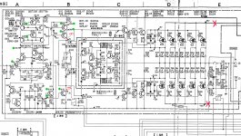
Please check the picture attached. The problem is the voltage at pre-driver BJTs bases which forms quiescent current. Should be +/-3v, but its showing almost the +rail voltage on both bases. My brain is smoking... green points are checked BJTs, all seems fine. Q112-Q115 base voltages also seems fine, but apparently Q113 and Q115 do not turn on.
Note: output stage rails for fets were cut, fets removed. I would really appreciate any ideas or some checking methodic.

Without the outputs, the NFB loop is open, at least if you don't temporarily tie the connection of R133 and R134 to the output bus. Thus the input LTP doesn't manage to adjust symmetry in any other part of the circuit. Why did you remove the power devices? What was the issue with your amp?
Best regards!
Best regards!
Last edited:
Well, as you can see the NFB loop is closed through R114-R115,
No, it isn't. Without the power devices the output bus is floating. Try connecting R132, R133, R134 and R178 to the output bus and report your measurements. They should roughly be the same as shown in your schematics.
I bet the service manual may contain some advice like this, as otherwise dividing the predrivers' and drivers' emitter resistors into two parts of tight tolerance doesn't make sense to me.
Best regards!
Last edited:
2SC2224 cannot have 5 volts between its base and emitter junction and survive!sure! all rails are fine. The most questioning thing for me is Q115, which has -105V at emitter, -100V at base and +92V at collector. Checked it twice with removing, BJT is OK.
2SC2224 cannot have 5 volts between its base and emitter junction and survive!
I gave rough numbers for simplicity. There's not 5V Ube but around 4.2V actually.
No, it isn't. Without the power devices the output bus is floating. Try connecting R132, R133, R134 and R178 to the output bus and report your measurements. They should roughly be the same as shown in your schematics.
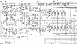
Just did all the above, as per the picture attached. No major changes, just +97V at Q113 collector gets down to +93V. Now suspect Q116 shortened collector to base, so will check all 6 driver devices.

Maximum Vbe is 0.72 Volts any more and the junction is destroyed. Have a look at the application note.I gave rough numbers for simplicity. There's not 5V Ube but around 4.2V actually.
Maximum Vbe is 0.72 Volts any more and the junction is destroyed. Have a look at the application note.
can't find the specsheet in google, but at least two links stating Ube as 5v max.
Nevertheless, I checked it twice out of the board with transistor checker and multimeter (have no curve tracer unfortunately).
If you have the specsheet please share.
The transistor is obsolete but silicon transistors have a junction voltage of about 0.7volts for ALL silicon transistors. The Vbe you have read is reverse bias voltage before the junction breaks down. The base voltage cannot be more positive with respect to the emitter than 0.7Volts. If it is then the junction and therefore transistor is damaged.
This only holds true for the reverse biased junction. Biased appropriately (conducting), Vbe is about .6V.can't find the specsheet in google, but at least two links stating Ube as 5v max.
Nevertheless, I checked it twice out of the board with transistor checker and multimeter (have no curve tracer unfortunately).
And it checked fine? What does your meter read for the aproppriate biased BE junction?
Best regards!
This is all I an find.
2SC2224 PDF Datasheet - American Microsemiconductor, Inc. - Datasheets360.com
2SC2224 PDF Datasheet - American Microsemiconductor, Inc. - Datasheets360.com
The transistor is obsolete but silicon transistors have a junction voltage of about 0.7volts for ALL silicon transistors. The Vbe you have read is reverse bias voltage before the junction breaks down. The base voltage cannot be more positive with respect to the emitter than 0.7Volts. If it is then the junction and therefore transistor is damaged.
True, will check this later. Meanwhile, whether its worth imitatating as if Q115 turns on with, say, 5-7k resistor across C-E, just to be sure that Q115 is totally off in current conditions? If reading at collector goes down significantly, then we understand Q115 is off, while according to schematics it should be definitely turned on.
Hi Arky,
I would do the following.
First of all, you need to make sure the front-end is working properly.
For that purpose, you need to:
- remove the pre-drivers Q116, Q119 (unsolder them carefully);
- jumper C111 with a piece of wire;
- connect the top of R119 with that shorted C111 through 5.6K resistor - that will form the complete NFB network.
Now you can power on the front-end - it will work as a voltage amplifier with 29db gain - shorted C111 as the output point.
If it works fine - we can move further, checking the driver stage.
If not - we need to troubleshoot the front-end.
Cheers,
Valery
Hi Arky,
I would do the following.
First of all, you need to make sure the front-end is working properly.
For that purpose, you need to:
- remove the pre-drivers Q116, Q119 (unsolder them carefully);
- jumper C111 with a piece of wire;
- connect the top of R119 with that shorted C111 through 5.6K resistor - that will form the complete NFB network.
Now you can power on the front-end - it will work as a voltage amplifier with 29db gain - shorted C111 as the output point.
If it works fine - we can move further, checking the driver stage.
If not - we need to troubleshoot the front-end.
Cheers,
Valery
OK thanks, will try.
Hi Arky,
I would do the following.
First of all, you need to make sure the front-end is working properly.
For that purpose, you need to:
- remove the pre-drivers Q116, Q119 (unsolder them carefully);
- jumper C111 with a piece of wire;
- connect the top of R119 with that shorted C111 through 5.6K resistor - that will form the complete NFB network.
Now you can power on the front-end - it will work as a voltage amplifier with 29db gain - shorted C111 as the output point.
If it works fine - we can move further, checking the driver stage.
If not - we need to troubleshoot the front-end.
Cheers,
Valery
shortened C111 reads +98V, however I can see some signal coming through. Q109 opposite base (top lead R119) reads +1.7V.
- Status
- This old topic is closed. If you want to reopen this topic, contact a moderator using the "Report Post" button.
- Home
- Amplifiers
- Solid State
- sony ta-n9 biasing