I've got an old HP3325B function generator, which does tolerable (-75dBc) sinewaves to 21MHz. It's a little dead at present (old caps), and I'm giving it a bit of a once-over.
Anyway, one of the options for the HP3325 is the "high voltage" option, which allows it to do 40Vpk-pk into 500 Ohms. I'd kinda like to do that. It involves a PCB with a gain of 4, that does DC to 1MHz.
I went looking for something that might get there in my simulations folder, and found the following topology:
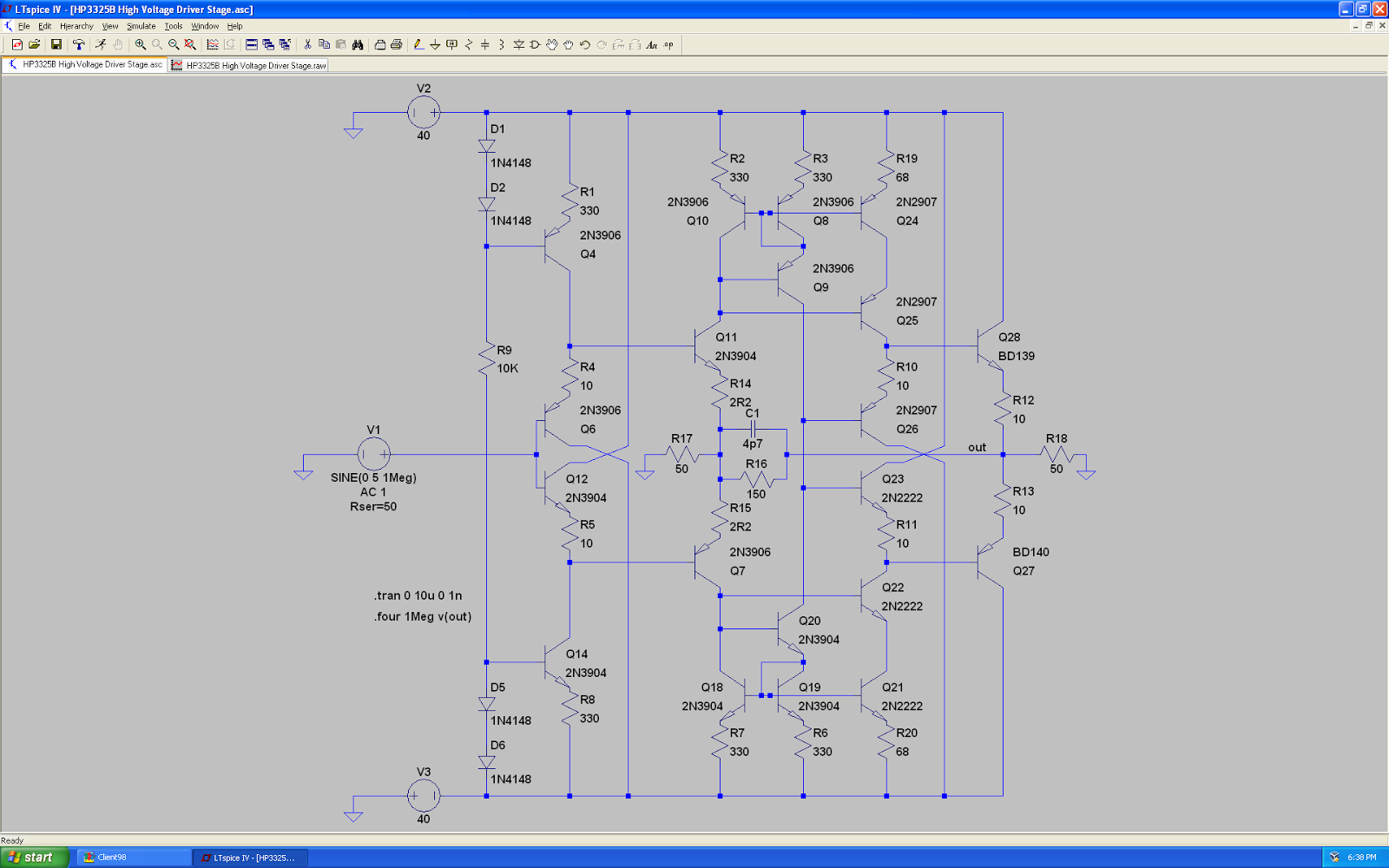
It's sort of a double-diamond with gain. I cannot for the life of me remember where I got it, but it's something of a screamer. I'm managing 0.08% pushing a 1 MHz 40Vpk-pk sinewave into 50 ohms, which is rather neat. At audio it does well, 0.001% full-stick at 10KHz. Wind the level back and it's straight away under 1ppm at 10KHz. 3dB roll-off is out beyond 100MHz.
Does anyone recognise it? I suspect it's the product of Per-Anders twisted mind, though I'm not discounting that I may have had some involvement.
Anyway, one of the options for the HP3325 is the "high voltage" option, which allows it to do 40Vpk-pk into 500 Ohms. I'd kinda like to do that. It involves a PCB with a gain of 4, that does DC to 1MHz.
I went looking for something that might get there in my simulations folder, and found the following topology:
It's sort of a double-diamond with gain. I cannot for the life of me remember where I got it, but it's something of a screamer. I'm managing 0.08% pushing a 1 MHz 40Vpk-pk sinewave into 50 ohms, which is rather neat. At audio it does well, 0.001% full-stick at 10KHz. Wind the level back and it's straight away under 1ppm at 10KHz. 3dB roll-off is out beyond 100MHz.
Does anyone recognise it? I suspect it's the product of Per-Anders twisted mind, though I'm not discounting that I may have had some involvement.
This is a current conveyor type of circuit similar to that found in CFA op-amps. Its principle of operation is quite simple. The input voltage is buffered by the diamond input buffer. The current drawn by the buffer's output (Q11, Q7) is mirrored into the high impedance point at the junction of the bases of Q23 and Q26. This provides the voltage gain, but as it is at a high impedance, an output diamond buffer is necessary. Feedback is taken from the circuit's output to the output of the input buffer, which is the inverting input.
Controlling the bandwidth with C1 is usually regarded as a no-no, as it can cause oscillation. The usual method of compensating these circuits is a capacitor to ground from the high impedance point (bases of Q23 and Q26). It should be possible to select a value which has the best bandwidth with no peaking at high frequencies.
These circuits have the interesting features that the bandwidth changes very little with changes to the gain, and there is no slew rate limitation caused by a Miller capacitor being charged by a fixed maximum current as is usually found in VFAs with feedback.
So these circuits are characterised by wide bandwidths and ultra-fast slewing. Their main disadvantage is that the inverting input is at a much lower impedance that the non-inverting input, which complicates life if one wants a differential input.
So these circuits are characterised by wide bandwidths and ultra-fast slewing. Their main disadvantage is that the inverting input is at a much lower impedance that the non-inverting input, which complicates life if one wants a differential input.
So, is this quite the same approach as in designs that are called CFA here?
Best regards!
So, is this quite the same approach as in designs that are called CFA here?
I think that if you read the literature on CFA's (see e.g. http://www.ti.com/lit/an/sloa021a/sloa021a.pdf), you will find that gain is always provided by a current conveyor, and this is certainly how they were originally conceived.
Having said that, there are amplifiers on this site described as CFA's in which gain is provided by a (dual) common emitter stage. On this view, perhaps the defining characteristic of a CFA is the low impedance of the inverting input. However, AFAIK all CFA integrated op-amps use a current conveyor to provide gain.
There is/was a very lively debate in this forum about VFA's v. CFA's, also Dadod's many excellent contributions to this forum are worth studying.
The topology is fairly straightforward and conventional, except for the clever bit, Q23 & Q26: they provide a clean and fast turnoff path to the OP devices, which must boost the HF performances significantly
Elvee, Q23 and Q26 are surely just part of the output buffer and a necessary and perfectly normal part of the CFA with current conveyor topology.
The unusual feature of the design is that the currents in Q23 and Q26 are not controlled by CCS's. Can you provide an insight into the function of Q24/Q25 and Q21/Q22?
Last edited:
I have a feeling that at full voltage output swing Q7 and Q11 will see very large
reverse Vbe that could damage the parts. I pointed this out several years ago
on the Tiger amps that are CFP with gain and recently on the Bryston 3B.
Might have to go into clipping to see the issue but I'm very curious to find out.
Otherwise I really like that design.
Looks like something from jcx, just guessing.
BJTs, as I understand it, are not designed to have any reverse Vbe, they become
noisy with degraded performance and then fail if the current is too much. I don't
know much more about this, anyone?
I think that if you read the literature on CFA's (see e.g. http://www.ti.com/lit/an/sloa021a/sloa021a.pdf), you will find that gain is always provided by a current conveyor...
AFAIK all CFA [IC] op-amps use a current conveyor...
I think you will find Current conveyor was common in early "CFA"s but many of the later implementations use a different structure.
For example, check US Patent 5,537,079 - held by AD and used in their op-amps, if Scot Wurcer is to be trusted
")
Best wishes
David
Referring firstly to the positive half...
...if I may? In the absence of exhaustive study and viewing this primarily from the perspective of what the designer was hoping to achieve:-
By way of their values R3 vs R19; Q24 produces a ~5x multiplier of the VAS mirror current from it's collector into R10. The other side of this is constrained by the emitter of Q26 at one Vbe up from the VAS output voltage. As this goes more positive greater current must be delivered into the base of Q28 to drive the load and in some proportion the relatively static cascode of Q25 provides this.
As always, NFB acts to ensure that V out remains directly proportional to the input. Meanwhile; in the negative half. Quiescent current in R13 reduces thereby increasing that available from the emitter of Q28 to flow into the load further reducing VAS current variation.
So one benefit of this topology is to prevent changes in output current from affecting the VAS and another is to further increase the output current available during each half cycle.
Additionally at high frequencies and with increasing amplitudes the multiplying mirrors appear intended to improve the circuit's responses by making larger currents available for the charge/discharge of the output stage's junction capacitances.
Whilst I have have not yet examined it for critical matching the intent of the designer seems moderately clear. I hope this cursory analysis is largely correct, reasonably entire and at least somewhat helpful?
Elvee, Q23 and Q26 are surely just part of the output buffer and a necessary and perfectly normal part of the CFA with current conveyor topology.
The unusual feature of the design is that the currents in Q23 and Q26 are not controlled by CCS's. Can you provide an insight into the function of Q24/Q25 and Q21/Q22?
...if I may? In the absence of exhaustive study and viewing this primarily from the perspective of what the designer was hoping to achieve:-
By way of their values R3 vs R19; Q24 produces a ~5x multiplier of the VAS mirror current from it's collector into R10. The other side of this is constrained by the emitter of Q26 at one Vbe up from the VAS output voltage. As this goes more positive greater current must be delivered into the base of Q28 to drive the load and in some proportion the relatively static cascode of Q25 provides this.
As always, NFB acts to ensure that V out remains directly proportional to the input. Meanwhile; in the negative half. Quiescent current in R13 reduces thereby increasing that available from the emitter of Q28 to flow into the load further reducing VAS current variation.
So one benefit of this topology is to prevent changes in output current from affecting the VAS and another is to further increase the output current available during each half cycle.
Additionally at high frequencies and with increasing amplitudes the multiplying mirrors appear intended to improve the circuit's responses by making larger currents available for the charge/discharge of the output stage's junction capacitances.
Whilst I have have not yet examined it for critical matching the intent of the designer seems moderately clear. I hope this cursory analysis is largely correct, reasonably entire and at least somewhat helpful?
In a plain vanilla amplifier, you would see an ordinary, passive base spreaderElvee, Q23 and Q26 are surely just part of the output buffer and a necessary and perfectly normal part of the CFA with current conveyor topology.
The unusual feature of the design is that the currents in Q23 and Q26 are not controlled by CCS's. Can you provide an insight into the function of Q24/Q25 and Q21/Q22
Q24 mirrors the amplified current from Q11, and is cascoded by Q26
...
For example, check US Patent 5,537,079 - held by AD...
Thanks for the reference, I'll check this out.
Q24 mirrors the amplified current from Q11, and is cascoded by Q26
Got it, thanks.
Hey how cool is this. It's the output stage from my 3325B:
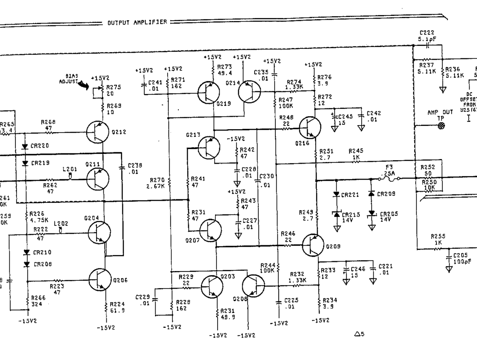
That schematic has a date of 1980 on it. I'd never heard of diamond buffers until the late nineties.
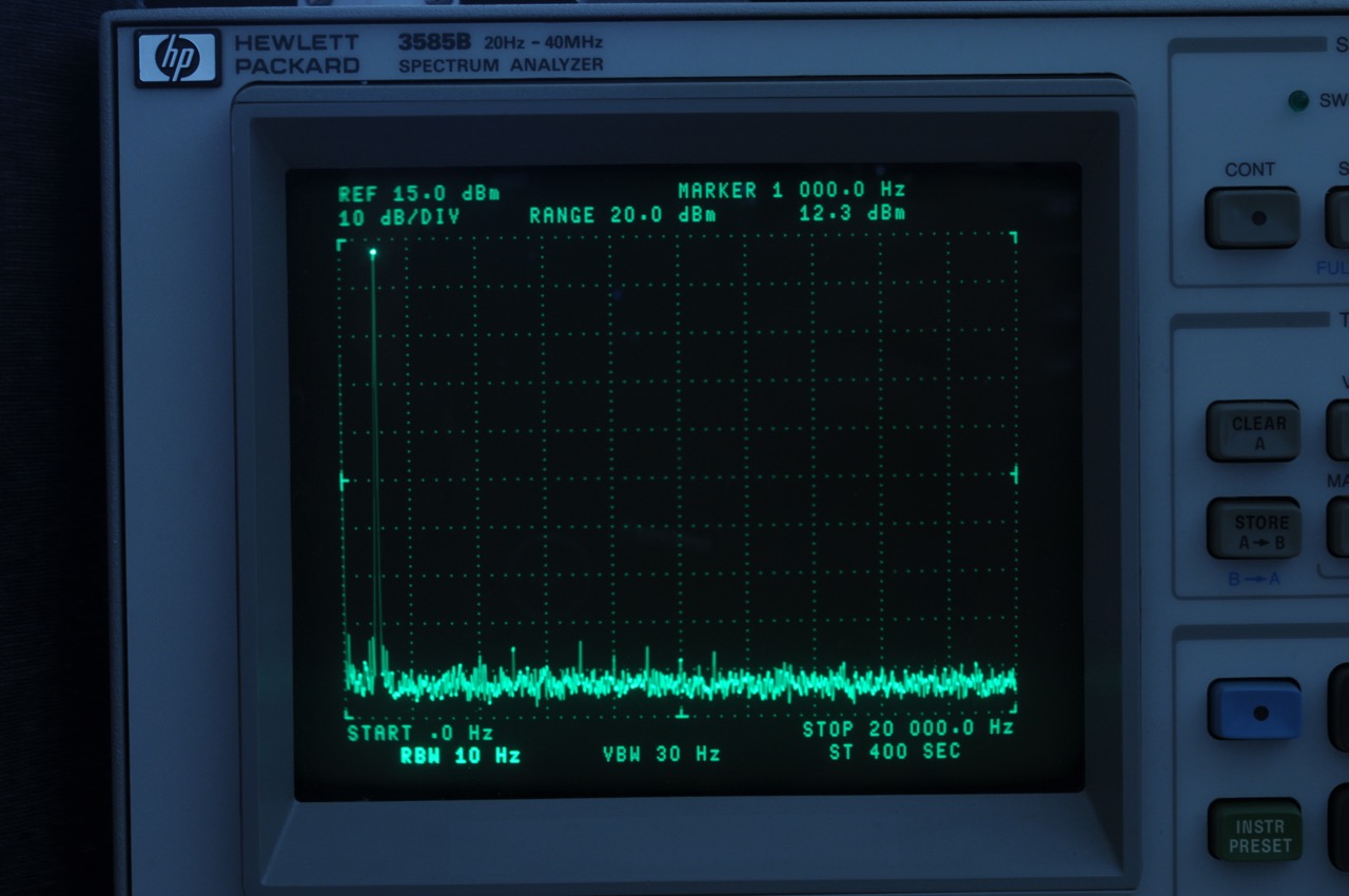
Also, much of the output distortion on my 3325 was down to a leaky tantalum at C245, which was messing up the bias of the output stage and introducing lots of even harmonic distortion. Replacing it, and then tweaking the mixer bias a little gives me better than 10dB improve in THD:
Next on the list is power supply caps - there's some horrid 100Hz ripple before the regulators that's getting through and causing intermods at the -80dBc level.
That schematic has a date of 1980 on it. I'd never heard of diamond buffers until the late nineties.
Also, much of the output distortion on my 3325 was down to a leaky tantalum at C245, which was messing up the bias of the output stage and introducing lots of even harmonic distortion. Replacing it, and then tweaking the mixer bias a little gives me better than 10dB improve in THD:
Next on the list is power supply caps - there's some horrid 100Hz ripple before the regulators that's getting through and causing intermods at the -80dBc level.
Last edited:
- Status
- This old topic is closed. If you want to reopen this topic, contact a moderator using the "Report Post" button.
- Home
- Amplifiers
- Solid State
- Does anyone recognise this topology?