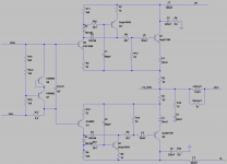
I've been designing this triple output stage with 3 goals:
UPDATE Sep. 2021: The latest version is in comment #14. The original version was probably not great, but we'll leave it here anyway.
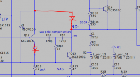
Only the predrivers need thermal compensation. The bias spreader uses two transistors, so each predriver can be thermally coupled to one of the bias spreader transistors.
C1 and C5 are frequency compensation caps. I set them where a 100kHz square wave looked the cleanest.
D1-D4 are baker clamps to keep the drivers out of saturation.
Superficially it looks like this design should be amenable to a "speed up" capacitor of 1uF across the bases of the outputs. I didn't have luck adding one; it tended to charge up during large signal outputs and leave the outputs temporarily over-biased.
The inductors here are supposed to model parasitics. The 0.001 ohm resistors are "Spice ammeters" so ignore those. Caveat simulator: I haven't built this yet.
Please critique this. Has it been done before? Surely nothing's really new under the sun.
- It needs no thermal sensing element on the heatsink, for ease of construction and reliability.
- It works with easily obtained outputs, even slowpokes like the MJ21195/6. (I have a heatsink that takes TO-3s and I'd rather not modify it, for ease of construction.)
- The complete amp makes inaudible distortion at all listening levels of course
")
UPDATE Sep. 2021: The latest version is in comment #14. The original version was probably not great, but we'll leave it here anyway.
Only the predrivers need thermal compensation. The bias spreader uses two transistors, so each predriver can be thermally coupled to one of the bias spreader transistors.
C1 and C5 are frequency compensation caps. I set them where a 100kHz square wave looked the cleanest.
D1-D4 are baker clamps to keep the drivers out of saturation.
Superficially it looks like this design should be amenable to a "speed up" capacitor of 1uF across the bases of the outputs. I didn't have luck adding one; it tended to charge up during large signal outputs and leave the outputs temporarily over-biased.
The inductors here are supposed to model parasitics. The 0.001 ohm resistors are "Spice ammeters" so ignore those. Caveat simulator: I haven't built this yet.
Please critique this. Has it been done before? Surely nothing's really new under the sun.
Attachments
Last edited:
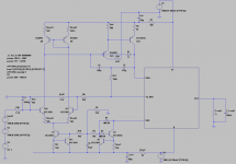
Here's a complete amp using this OPS.
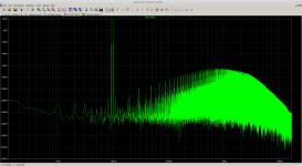
The simulated signal-to-distortion ratio is better than 110db at any level, measured using 9kHz + 10kHz input sinewaves. That's looking at audio-spectrum distortion products only. Ultrasonics aren't too bad either, the MHz-range distortion products are 85 or 90db below signal.
I've been setting the bias at about 10mA through the outputs. Bias is fixed at about 25mA through the drivers, so there's a grand total of 35mA through the ballast resistors.
Distortion performance suffers if bias current is too high (>40mA through the outputs.) Spice doesn't show any reduction in distortion performance at very low bias currents at the outputs, probably because the drivers still have some bias current flowing in R13 and R14 and can drive the output rail until the outputs turn on. The FFT shows -115db distortion even with zero output bias current, and yet there are visible crossover artifacts in this mode, an odd combination too see together! The zero crossing artifacts vanish with just a few mA of bias current in the outputs.
There doesn't seem to be any benefit from current limiting the VAS. This OPS isn't prone to draw high currents from the VAS at clip.
Attachments
Last edited:
I think your solution is very - too - difficult. Why not use the configuration of the Audiolab 8000A, which is a EF-CFP configuration with 3 transistors.
Why? The OP's design basically resembles a double Sziklai, or cascaded Sziklai (NPN-PNP-NPN for the positive, and PNP-NPN-PNP for the negative half, respectively), whose power devices easily can be paralleled, as the OP shows in #4. The Audiolab configuration's power devices are quasi common collector. So, if you want (or need) to provide more pairs, you need to have to add emitter resistors, one for each device. These will introduce additional voltage - and thus power - loss.
Btw, I don't understand the OP's claim that no thermal coupling between the Vbe multiplier and the power devices is necessary. Could someone please explain?
Thanks and best regards!
I think your solution is very - too - difficult. Why not use the configuration of the Audiolab 8000A, which is a EF-CFP configuration with 3 transistors.
Marc.
Audiolab utilizes a completely different arrangement from the one we discuss.
CFP-EF, presented by the OP makes a lot of sense.
Is it intended to be a class AB amp?
I built a "triple output" version some decades ago. It was a Danish "no feedback" amplifier. Well it had feedback but no global NFB. The name of it was "The end" ( good name )
I didn't like the sound of it. And I think the culprit was that triple configuration. I think it worsens cross over dist since the two halves are turning on and off quite sharply, since there are two independent feedback loops.
These kind of circuits should be run in class A, I think.
I talked about that DIY amp ( The end) with a guy at a local hifi store. One of the staff had actually built one and everyone agreed that any simple NAD amp outperformed it sonically.
But perhaps your amp will be the first good one.
jpc2001,
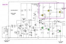
When I saw your schematic it looked familiar, and after some searching through my collection of schematics I found the Quad 303 (see attachment). The Quad used a similar circuit as the positive portion of a Quasi style amp, and I believe the Quad 303 was a reasonable amp. Note the very low quiescent current of 10mA.
regards,
Paul Bysouth
Attachments
Kay,
The bias voltage spans the predriver B-E junction, the predriver degeneration resistors, and the ballast resistors, nothing else. If the outputs' Vbe drifts, the predrivers should react to keep nearly-constant voltage across the ballast resistors.
In spice you can change the type of output transistor without adjusting the bias -- something that rarely works with an EF, as each type has a somewhat different Vbe drop.
Svitjod,
This is a class AB amp. Crossover distortion is a concern. None of the output stage is class A, turn-on and turn-off are abrupt. Emitter degeneration on the predrivers smooths this a little bit.
Paul,
Thank you! The 303 has a good reputation, let's shamelessly copy it! \o/
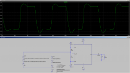
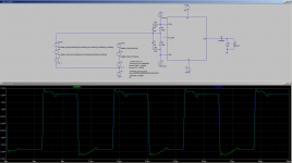
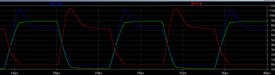
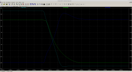
The designs posted above have serious cross-conduction issues on the 100kHz square wave test.
The red and blue lines here show the current through the output transistor emitters; notice how they jump up together on each edge. That looks destructive.
The red and blue lines here show the current through the output transistor emitters; notice how they jump up together on each edge. That looks destructive.
Attachments
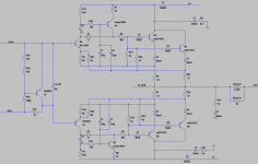
minor redesign
This redesign reduces cross-conduction by adding 2 small signal transistors per channel.
The new transistors can turn-off the drivers quite fast. The drivers turn-on more slowly, through a fairly stiff resistor. Under sharp transients, opposing drivers are now unlikely to both switch on.
I also lightened the compensation. The new OPS has some peaking in its standalone frequency response. This is several octaves above the TMC transition frequency where it doesn't seem to hurt the overall amplifier's stability.
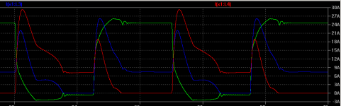
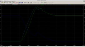
Cross conduction is mostly reduced, and what remains looks less destructive. Again, the outputs' emitter currents is shown below in red and blue, in a 100kHz square wave test.
This redesign reduces cross-conduction by adding 2 small signal transistors per channel.
The new transistors can turn-off the drivers quite fast. The drivers turn-on more slowly, through a fairly stiff resistor. Under sharp transients, opposing drivers are now unlikely to both switch on.
I also lightened the compensation. The new OPS has some peaking in its standalone frequency response. This is several octaves above the TMC transition frequency where it doesn't seem to hurt the overall amplifier's stability.
Cross conduction is mostly reduced, and what remains looks less destructive. Again, the outputs' emitter currents is shown below in red and blue, in a 100kHz square wave test.
Attachments
Here's a complete amplifier using a refined version of the same OPS above. The frontend and VAS are adapted from the new Wolverine. It simulates to about -129dB distortion in-band with ample stability margins.
Why CFP:
This amplifier has a few other nice features:
Why CFP:
- Saves power: optimal bias has each output device dissipating only about 2W.
- When your driver board is here and the heatsink is over there, wiring the thermal compensation transistor on the heatsink can be tricky: if any lead opens, bias current goes to infinity. If you're lucky you only blow a fuse. This OPS does not need thermal compensation for the outputs, only the drivers and predrivers need to be thermally coupled to the bias transistor. All thermal compensation is local to the driver board.
- Allows slightly lower in-band distortion than EF3.
This amplifier has a few other nice features:
- Input impedance is boosted with R15 "bootstrapped" to the NFB network. Old Yamaha amps did this. Allows the use of a lower-impedance NFB network without reducing input impedance. Allows the use of a smaller DC-blocker cap in the input network.
- The TPC resistor returns to the VAS emitter instead of ground. This removes some distortion and some supply ripple from the current that the IPS must feed to C4A.
- The current mirror returns to the VAS emitter instead of to the negative rail. This minimizes the voltage "bounce" across the cascode's outputs and also across the mirror's collectors.
- Cascoded VAS buffer, stolen directly from the new Wolverine.
- The lag network (C1 and R2) at the VAS output tames the in-band loopgain peak that TPC would otherwise produce. Unlike the TPC "bridge" capacitor, this approach doesn't bring any distortion from the VAS output back to the load on the IPS.
- A 2nd-order RF filter at the input cancels out the ~300kHz closed-loop frequency response peak that TPC would otherwise produce. And it should be better at filtering actual RF.
- The OPS is stabilized at HF by C8, C10, R34 and R35. At LF these are high impedance and the CFP feedback loop includes the outputs. At HF, the CFP feedback loop changes to only encompass the drivers.
- CFP bias spreader, since bias precision is more important for a CFP OPS than EF2/3. With luck this will allow setting the bias on the dim-bulb tester and then still having it be correct or quite close at full wall voltage.
Attachments
Last edited:
I did also look into this at The (New) Approach to Maximize NFB Around Output Devices
In your version, you get feedback before Re of output transistors, which is good for bias control.
For me, I would rather get feedback from entire output. It results much lower THD. I put bias control right before output devices and use traditional way to thermal compensation. Although the traditional thermal compensation is not perfect, it still works.
I note this triple output stage topology isn't new, Doug Self mentions it being used in a 1975 Lecson amp (AP-1). In his "Audio Power Amplifier Desgin" 6th ed. its shown in fig 9.17(a).
He mentions stability is an issue and significant emitter-degeneration is pretty much required in the first devices of the triple to tame it. Note that the loop-gain internal to this triple can be huge due to the two common-emitter stages.
He mentions stability is an issue and significant emitter-degeneration is pretty much required in the first devices of the triple to tame it. Note that the loop-gain internal to this triple can be huge due to the two common-emitter stages.
fixing cross conduction
Made a few updates since comment 14 to reduce cross conduction--
With a really abusive load like a 10uF cap (is there a better model of electrostatic speakers?) the OPS still rings and cross-conducts during the squarewave test. I doubt any CFP OPS is a good candidate for electrostatics. The Quad 303 that uses a similar OPS was purpose built to drive electrostatics. But that amp was AC coupled. It had an output inductor and then a 2000uF output capacitor with probably an ohm of ESR to protect the amp.
The target for this amp is 4-ohm dynamic speakers, and it's solid with them.
Made a few updates since comment 14 to reduce cross conduction--
- Removed the 1uF "speedup" cap from the output stage, to avoid the risk it could charge up and cause cross-conduction. This increases ultrasonic distortion products but in-band is no worse.
- Limited slew rate to ~20V/usec. The VAS from the comment 14 circuit can slew negative VERY fast and that gets us in trouble: on a fast negative-edge squarewave, the PNP outputs start conducting before the NPNs can turn off and there is brief cross-conduction.
- The slew-rate-limit is implemented by Dslew1 which conducts only during fast negative slew. It makes the IPS discharge Ctpc2, and the IPS has only ~3mA available, setting the slew rate limit. Rslew1 and Cslew1 bias the center of the TPC network to reverse-bias Dslew1 in normal operation. There might be a more elegant way to limit the slew rate -- but this seems to work and doesn't reduce distortion performance.
With a really abusive load like a 10uF cap (is there a better model of electrostatic speakers?) the OPS still rings and cross-conducts during the squarewave test. I doubt any CFP OPS is a good candidate for electrostatics. The Quad 303 that uses a similar OPS was purpose built to drive electrostatics. But that amp was AC coupled. It had an output inductor and then a 2000uF output capacitor with probably an ohm of ESR to protect the amp.
The target for this amp is 4-ohm dynamic speakers, and it's solid with them.
Attachments
cross conduction with nasty squarewaves
Here's the fast slew squarewave test into a 3.2 ohm resistive load. These plots show the output rail and current through one ballast resistor on each side of the OPS.
I don't know if there's a rule of thumb about how much cross conduction is too much. But these don't look bad. Overshoot is minimal. Total current during worst-case cross-conduction is not much more than the steady-state current during the square wave "plateau". And everything settles out within ~5usec.
Attachments
- Home
- Amplifiers
- Solid State
- novel(?) CFP triple output stage