I'm trying to get a good estimate of the needed resistance of ballast resistors when paralleling a bank of output BJTs. I'm not sure if I'm looking at this the right way (trying to do a maybe too-simplified estimate?), would appreciate any direction others here may have. Hoping to avoid trying to dredge up semiconductor physics. Anyone want to slog through this? Or can the correct calculation for this be found somewhere I haven't looked?
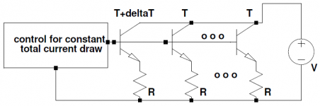
Here's the situation: Two (or more) BJTs, all have their collectors tied together, their bases tied together, and each emitters has its own ballast resistor R to a common emitter point. The collector voltage is constant above the common emitter voltage and the whole set is controlled (via the base to the common emitter voltage) to regulate the total current.
One of the BJTs gets a little hotter (deltaT degrees) than the others, and the ballast value needs to be large enough to prevent the hot transistor from going into thermal runaway.
The extra temperature results in the Vbe of the hot transistor to tend to drop (approximately, according to Ebers-Moll model) 2mV for every degree K that its heat exceeds that of the others. Which if unregulated, would increase the drop across resistor R and cause an increase in that transistor's current of about 2m*deltaT/R. But since the total current of the whole bank is being regulated, it doesn't go quite that high -- if there are two in the bank, one would increase by approximately 1m*deltaT/R, the other would decrease by that amount. (If the bank has more than two transistors in it, then the current increase of the hot transistor would be something like (1-1/N)*2m*deltaT/R. I think.).
So assuming that is approximately right, and only two devices in the bank (for example) then the additional power dissipation of that transistor would be about Vce*1m*deltaT/R. The junction will have a thermal resistance between it and the heatsink of Theta. The total power of the bank doesn't change so the heatsink temperature should stay about the same (neglecting thermal resistance between the devices where they mount -- is that a big mistake to assume?). So the Theta of interest is the Theta(jc) [K/W] of the package plus the thermal resistance of the package to the heatsink.
The extra power should raise the junction temperature again by Theta*Vce*1m*deltaT/R. In order to not run away infinitely (edit: actually, not infinitely, only till it hogs all the current), this has to stay lower than the deltaT that started the whole change. So, require that:
Is that anywhere near correct? I can see one (mitigating) factor that is not included, which is the internal resistance that might already exist in each emitter leg. And if the overall heatsink temp doesn't rise about the same for each BJT, that would also skew the calculation (probably would be an addition to the Theta value).
A concern is that using this calculation, I get R values quite a bit smaller than I'd expect and usually see (is that to allow for the possibility of a weaker thermal interface on one of the devices from the others -- to avoid failure from one misapplied bit of thermal goo?). Or is this approach just too simplistic, or did I miss something? What's the right way? Set me straight.
Here's the situation: Two (or more) BJTs, all have their collectors tied together, their bases tied together, and each emitters has its own ballast resistor R to a common emitter point. The collector voltage is constant above the common emitter voltage and the whole set is controlled (via the base to the common emitter voltage) to regulate the total current.
One of the BJTs gets a little hotter (deltaT degrees) than the others, and the ballast value needs to be large enough to prevent the hot transistor from going into thermal runaway.
The extra temperature results in the Vbe of the hot transistor to tend to drop (approximately, according to Ebers-Moll model) 2mV for every degree K that its heat exceeds that of the others. Which if unregulated, would increase the drop across resistor R and cause an increase in that transistor's current of about 2m*deltaT/R. But since the total current of the whole bank is being regulated, it doesn't go quite that high -- if there are two in the bank, one would increase by approximately 1m*deltaT/R, the other would decrease by that amount. (If the bank has more than two transistors in it, then the current increase of the hot transistor would be something like (1-1/N)*2m*deltaT/R. I think.).
So assuming that is approximately right, and only two devices in the bank (for example) then the additional power dissipation of that transistor would be about Vce*1m*deltaT/R. The junction will have a thermal resistance between it and the heatsink of Theta. The total power of the bank doesn't change so the heatsink temperature should stay about the same (neglecting thermal resistance between the devices where they mount -- is that a big mistake to assume?). So the Theta of interest is the Theta(jc) [K/W] of the package plus the thermal resistance of the package to the heatsink.
The extra power should raise the junction temperature again by Theta*Vce*1m*deltaT/R. In order to not run away infinitely (edit: actually, not infinitely, only till it hogs all the current), this has to stay lower than the deltaT that started the whole change. So, require that:
Theta*Vce*1m*deltaT/R < deltaT
R > (Theta*Vce*1m/R)
Adjust the 1m value above as needed for more than 2 devices used in the bank. And of course R would have to be significantly bigger than the resulting value, since the calculation is for when it just barely doesn't take off.R > (Theta*Vce*1m/R)
Is that anywhere near correct? I can see one (mitigating) factor that is not included, which is the internal resistance that might already exist in each emitter leg. And if the overall heatsink temp doesn't rise about the same for each BJT, that would also skew the calculation (probably would be an addition to the Theta value).
A concern is that using this calculation, I get R values quite a bit smaller than I'd expect and usually see (is that to allow for the possibility of a weaker thermal interface on one of the devices from the others -- to avoid failure from one misapplied bit of thermal goo?). Or is this approach just too simplistic, or did I miss something? What's the right way? Set me straight.
Attachments
Last edited:
I think you need to tighten this criterion. Think of it as a positive feedback loop (which is what it is!). Loop gain less than 1 ensures stability, but you need even less gain to avoid significant excursions when disturbed. In AC terms you don't just want the loop to be stable, but you also want to avoid significant ringing. Off the top of my head, I would take the result of your calculation and at least double the resistor value.bwaslo said:The extra power should raise the junction temperature again by Theta*Vce*1m*deltaT/R. In order to not run away infinitely, this has to stay lower than the deltaT that started the whole change.
Double sounds like a decent margin for error. I agree that the R calculated only results in preventing total thermal runaway. Or, at least up to where the one hot device draws ALL the current... I guess that's an asymptotic limit to it, and the junction temperature would reach some sort of equilibrium regardless.
But in this scenario (which is an actual real situtation), I'm not concerned about "ringing" (at least not ringing of the current) as the total current doesn't change and the temperature/individual-current difference will only ever be toward increasing. But too much "positive feedback" into the thermal runaway mechanism will make the "hot" device creep up to to be still hotter (than the other devices) than if the "positive feedback" were less. But I can't see a way to quantify how much.
I don't use actual calculus a lot anymore, but can't see a way to quantify the limit from what calculus I do remember. But surely there must be a way.
Last edited:
LTSPICE allows you to individually set the temperature of each circuit element. The three transistors can be at three different temperatures and the three emitter resistors can be at three other different temperatures.
Maybe you can set one transistor's temperature to be 5 degrees C hotter than the other two transistors (giving a VBE offest voltage of 10mV) and observe the simulated power dissipation of each device. Monkey around with emitter resistance values until you get results you can live with. Then multiply by a safety guardband (150% ??) because you worry that LTSPICE is a big fat liar.
Maybe you can set one transistor's temperature to be 5 degrees C hotter than the other two transistors (giving a VBE offest voltage of 10mV) and observe the simulated power dissipation of each device. Monkey around with emitter resistance values until you get results you can live with. Then multiply by a safety guardband (150% ??) because you worry that LTSPICE is a big fat liar.
Attachments
Mark, thanks for suggesting that approach. I forgot about LTSPICE allowing setting of the individual temperatures. I'll give that a try.
It does still bug me that I can't see a direction to estimate this with algebra or calculus, just on the intellectual question!
Edit: on second thought, how would that include the extra heating caused by the current change (cascading effect)?
It does still bug me that I can't see a direction to estimate this with algebra or calculus, just on the intellectual question!
Edit: on second thought, how would that include the extra heating caused by the current change (cascading effect)?
Can I set the temperature of each device in LTSPICE via a formula (i.e., T_heatsink + power_dissipation * Theta)?
Spice works on simultaneous equations (matrices), I should be able to set that up on paper, all the simplified assumptions are for linear behaviours. After a little more morning coffee, that is (slept late!)
Spice works on simultaneous equations (matrices), I should be able to set that up on paper, all the simplified assumptions are for linear behaviours. After a little more morning coffee, that is (slept late!)
Last edited:
I think this is solvable with math using a system of differential equations for the heat transfer. You could make some assumptions like a uniform heat sink temperature, assume a mass and thermal conductivity of the transistor to heatsink junction. Each transistor is a heat source given by the equations of dissipation (electrical), then heat carried off by fins and radiated via natural convection needs to be assumed per rating of sink. You could make it complex by adding transistor to transistor conduction and not assuming uniform heatsink. Mathcad or Matlab will almost be essential to solving this. Although it could be modeled as lumped elements as resistor and capacitor networks and all done in LTSpice.
Check out this publication from Infineon, Figs. 8 and 9 in particular to see clues of how to go about this. It shows coupled electrical and thermal models for 1 MOSFET. Now add second and coupling between two via thermal model of heatsink.
http://www.infineon.com/dgdl/Thermal+Modeling.pdf?fileId=db3a30431441fb5d011472fd33c70aa3
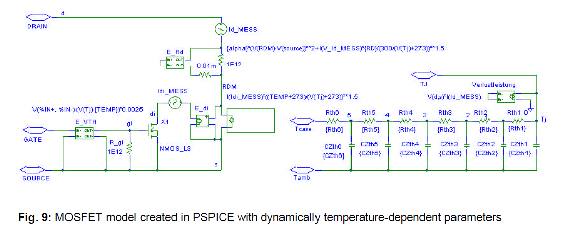
Fig. 13 is good too.
Check out this publication from Infineon, Figs. 8 and 9 in particular to see clues of how to go about this. It shows coupled electrical and thermal models for 1 MOSFET. Now add second and coupling between two via thermal model of heatsink.
http://www.infineon.com/dgdl/Thermal+Modeling.pdf?fileId=db3a30431441fb5d011472fd33c70aa3
Fig. 13 is good too.
Attachments

Last edited:
Something that just occurred to me: if I'm to set this up in simultaneous equations or SPICE, there has to be something that starts the temperature difference between the devices. If all are the same, then so are the temperatures. So I guess I have to assign a cause by varying something in one of the BJTs ( I(S)? That would send things right off non-linear).
Maybe better to give one of them a slightly different Theta to the heatsink?
Maybe better to give one of them a slightly different Theta to the heatsink?
I think you need to ask what is different in the samples of different transistors, the important things, as I see it, are Vbe and beta. You could probably simulate Vbe differences in the transistors by adding a DC source in the base, or emitter, have not thought about it enough to think if one is better, and then you'll see differences in the currents which will start one heating more than the others. I think you'll also see that as you raise Re, the change from the DC source has less effect and they share more evenly.
It sounds like you built this, do you have any chance of getting power transistors from the same wafer, or same lot? Look at the date codes.
It sounds like you built this, do you have any chance of getting power transistors from the same wafer, or same lot? Look at the date codes.
Thanks. I've built similar, but I want a way to calculate rather than just changing resistors in each particular design iteration until something stops overheating. So I can come up with an R value before building, that is.
It seems that something like this scenario occurs a lot in power amps -- assuming something to keep the total idle current in check but only the ballast resistors to keep things somewhat balanced. Everyone seems to use something around 0.1 ohms to 0.68 ohms for R, but I can't find where that comes from. I was also wondering whether the actual current magnitude affects this (i.e., do higher bias currents such as class A allow for smaller values of R or need larger values of R, or does it matter?)
It seems that something like this scenario occurs a lot in power amps -- assuming something to keep the total idle current in check but only the ballast resistors to keep things somewhat balanced. Everyone seems to use something around 0.1 ohms to 0.68 ohms for R, but I can't find where that comes from. I was also wondering whether the actual current magnitude affects this (i.e., do higher bias currents such as class A allow for smaller values of R or need larger values of R, or does it matter?)
Intuitively I would say, having 0.68 as Re, a difference of 1A between a pair would cut off one of them completely wrt the other. So that appears a limit case. What you need is a way to graph this and you can then hopefully empirically read the values from a graph. I think.
Maybe one assumption is the max delta-Ic you would allow and work from that. Just thinking out loud.
Jan
Maybe one assumption is the max delta-Ic you would allow and work from that. Just thinking out loud.
Jan
")
Just assume that the BJTs have slightly different VBEs. You know, input offset voltage. Manufacturing variation. Murphy's Law.
Why? Because the BJTs came from different places on the wafer and received slightly different implant depths.
Insert a 5mV independent voltage source in series with one base terminal.
Why? Because the BJTs came from different places on the wafer and received slightly different implant depths.
Insert a 5mV independent voltage source in series with one base terminal.
We still need to include the mechanism where the heating changes the current which changes the heating
I was just thinking of showing how Re reduces the Ic mismatch not trying to
simulate the actual change. I thought you just wanted to know how much
Re you needed.
I have not put a lot of thought into this but I seem to remember someone simulating
device temps, can't remember where at the moment.
Functional solution?
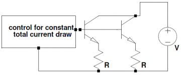
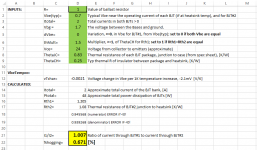
Ok, here's a new calculation, and a spreadsheet intended to predict results for given values of circuit parameters. This is for NPN devices, per the drawing below.
Assume that:
The value of interest is I1/I2, or the percentage that I1 exceeds I2. IOW, current hogging!
The current in either BJT is the voltage across its resistor R, divided by R. The power dissipation in either BJT is its current times Vce. The temperature of each junction rises above the heatsink temp by an amount equal to the power dissipation times its Rth, which causes a corresponding decrease in its Vbe. So
If you buy all these approximations, then a few things of note:
1) If the Rth values are equal, then the result doesn't depend on that value of Rth, but can depend on the operating current.
2) If the Vbe values are equal, then the result doesn't depend on the operating current.
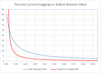
See the attached spreadsheet if you want to play with the relationships. Attached is a graph of a situation I'm looking at with Vce~= 24V, Itotal = 2A, ThetaJC=0.83K/W, ThetaCH=0.25K/W. The y axis is "% hogging", the x axis is the value of R. The blue curve is for an assumed decrease of 25mV for Vbe of BJT#1 (I don't know how realistic that is, unfortunately). The red curve is for an assumed increase of 50% for the thermal resistance of the Case to Heatsink for BJT#1 (might be about right for too much grease or a lump?).
Does anyone have a handle on what kind of typical variation might be expected for Vbe in a batch of unselected power transistors? Does the approach seem reasonable?
Ok, here's a new calculation, and a spreadsheet intended to predict results for given values of circuit parameters. This is for NPN devices, per the drawing below.
Assume that:
- Vbe(typ) is typical Vbe for linear operation if at the heatsink temp, somewhere around 0.7V
- Itotal is the approximate total current for the bank of bipolar transistors
- Vbg is the voltage between the bases and the lower net on the drawing
- dVbe is the voltage variation that BJT#1 has in Vbe, relative to Vbe(typ). (<=0)
- Vbe2 (for BJT#2) is assumed to be Vbe(typ); Vbe1 is assumed to be Vbe1+dVbe.
- ThetaJC is the thermal resistance of each BJT package (assumed equal)
- ThetaCH is the typical thermal resistance from package to heatsink
- thMult is a multiplier on ThetaCH, for BJT#1 (>=1)
- Rth1 is the sum of thermal resistances for BJT#1, equals ThetaJC+ThetaCH*thMult
- Rth2 is the sum of thermal resistances for BJT#2, equals ThetaJC+ThetaCH
- Vce is the approximate Collector-Emitter voltage of the BJTS (>1), assumed close enough to equal for all
- I1 is the emitter current of BJT#1
- I2 is the emitter current of BJT#2
- base currents are ignored
- Vbe varies by -2.1mV/K of the junction temp;
The value of interest is I1/I2, or the percentage that I1 exceeds I2. IOW, current hogging!
The current in either BJT is the voltage across its resistor R, divided by R. The power dissipation in either BJT is its current times Vce. The temperature of each junction rises above the heatsink temp by an amount equal to the power dissipation times its Rth, which causes a corresponding decrease in its Vbe. So
I(N) = [(Vbg-Vbe(N)-2.1E-3*(I(N)*Vce*Rth(N)]/R or
I(N) = (Vbg - Vbe(N))/(R - 2.1E-3 * Vce * Rth(N))
then
I1/I2 = (Vbg-Vbe1)*(R - 2.1E-3 * Vce * Rth2)/((Vbg-Vbe2)*(R - 2.1E-3 * Vce * Rth1))
I(N) = (Vbg - Vbe(N))/(R - 2.1E-3 * Vce * Rth(N))
then
I1/I2 = (Vbg-Vbe1)*(R - 2.1E-3 * Vce * Rth2)/((Vbg-Vbe2)*(R - 2.1E-3 * Vce * Rth1))
If you buy all these approximations, then a few things of note:
1) If the Rth values are equal, then the result doesn't depend on that value of Rth, but can depend on the operating current.
2) If the Vbe values are equal, then the result doesn't depend on the operating current.
See the attached spreadsheet if you want to play with the relationships. Attached is a graph of a situation I'm looking at with Vce~= 24V, Itotal = 2A, ThetaJC=0.83K/W, ThetaCH=0.25K/W. The y axis is "% hogging", the x axis is the value of R. The blue curve is for an assumed decrease of 25mV for Vbe of BJT#1 (I don't know how realistic that is, unfortunately). The red curve is for an assumed increase of 50% for the thermal resistance of the Case to Heatsink for BJT#1 (might be about right for too much grease or a lump?).
Does anyone have a handle on what kind of typical variation might be expected for Vbe in a batch of unselected power transistors? Does the approach seem reasonable?
Attachments
Last edited:
You have derived a formula for the temperature rise caused by a temperature rise. All you have to do is put this result in the form of the normal feedback equation (for positive feedback), then you can see what the effect will actually be for a given initial fluctuation or imbalance. I think you will find that if you choose a resistor twice the calculated value, then the temperature deviation will be twice the stimulus. Three times the calculated value gives 150% of the stimulus etc.
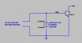
I tested twelve Fairchild D44H11 power transistors from lot code "C20AB" using the test fixture illustrated below. It took fifteen minutes.
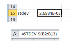
The sample standard deviation of "VBE" was 2.69 millivolts. I will let other readers consider how to turn that into an estimate of the population standard deviation. Want raw data? Spend fifteen minutes measuring.
The sample standard deviation of "VBE" was 2.69 millivolts. I will let other readers consider how to turn that into an estimate of the population standard deviation. Want raw data? Spend fifteen minutes measuring.
Attachments
- Status
- This old topic is closed. If you want to reopen this topic, contact a moderator using the "Report Post" button.
- Home
- Amplifiers
- Solid State
- About the math of paralleled power transistors and current hogging