Hi. This is my first amp design and I don't know much about amplifiers or analog electronics.
This project was made mostly for fun and learning, trying to use common components and make it inexpensive. I intend to use it with low power speakers (2x 3W and maybe a 9W sub I have around here). It's made with single supply in mind, as I have some transformers with only two output wires around here.
I would like to know where, how and why I could improve this design, or if it's total rubbish. It looks alright to me.
Thanks a lot. :3


View attachment kamp.asc
This project was made mostly for fun and learning, trying to use common components and make it inexpensive. I intend to use it with low power speakers (2x 3W and maybe a 9W sub I have around here). It's made with single supply in mind, as I have some transformers with only two output wires around here.
I would like to know where, how and why I could improve this design, or if it's total rubbish. It looks alright to me.
Thanks a lot. :3
View attachment kamp.asc
Drivers and Vbe need to thermally interact so TO-92 isn't the best choice for those parts.
Power target is a little ambitious for those output devices. If you need 4 ohm driving capability from a 12V supply, I suggest at least the MJE340/350 as outputs, they can take a bit more abuse.
You will also need some stability components. A lot of them, in fact. The input will need one as well as the lower driver. Both is advisable.
Can you explain further about drivers and Vbe? You are talking about Q1 and Q2, right?
I don't need to use 12V it can be higher or lower voltage. BD140/139 are really common, but it seems I can find MJE340/350 around here too.
Can you explain further about these stability components?
Thanks.
I don't need to use 12V it can be higher or lower voltage. BD140/139 are really common, but it seems I can find MJE340/350 around here too.
Can you explain further about these stability components?
Thanks.
Useful though the MJE devices are, they are definitely not suited to output stage duty having a very low 0.5amp Ic. The BD139/140 are better in that regard.
TIP31/TIP32 or TIP41/42 would be a much better choice.
Thermal compensation for the Cfp configuration (complementary feedback pair) require the drivers (at least one of them) to be in thermal contact with the vbe multiplier rather than an output transistor in contact with the multiplier in an emitter follower type stage.
The resistive biasing at the input isn't ideal because any noise etc on the 12 volt rail will couple into the amplifier input. A simple zener reference of say 8.2 volts and a preset across that to trim the midpoint voltage would be much better imo.
You might want to look at taming the hf response a little and perhaps adding an input rf filter.
It looks basically all OK though. Oh, and a higher rail would make a massive improvement.
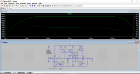
Have a look at this. Remember I thought the hf response needed taming. Well this is how it looked on squarewave testing. The 15pf cap neatly tames this behaviour. The current in the VAS stage is increased slightly... 2ma was to low. The zener shows the kind of set up I was referring to.
I'm not saying its perfect but it addresses a couple of issues. Good work though")
I'm not saying its perfect but it addresses a couple of issues. Good work though
Attachments
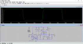
Nice, it greatly improved the frequency response. Why did you chose that node to attach the capacitor to the feedback?
About the drivers and Vbe multiplier transistors being in thermal contact, should I attach them directly to a metal tab? Or just leaving them near each other enough?
The zener was a good idea.
Thanks a lot.
About the drivers and Vbe multiplier transistors being in thermal contact, should I attach them directly to a metal tab? Or just leaving them near each other enough?
The zener was a good idea.
Thanks a lot.
If the circuit allows I tend to prefer that method of feedback as it doesn't add to any slew type induced distortion generated from the output stage.
Ideally the driver/s should contact the multiplier but you have to be practical and ask yourself whether you are aiming for milliamp precision stability or whether a modest drift in bias vs temperature is acceptable. The multiplier can be attached via trailing wires and glued etc to the best location (I increased the cap over the multiplier to a 10uf electrolytic).
Ideally the driver/s should contact the multiplier but you have to be practical and ask yourself whether you are aiming for milliamp precision stability or whether a modest drift in bias vs temperature is acceptable. The multiplier can be attached via trailing wires and glued etc to the best location (I increased the cap over the multiplier to a 10uf electrolytic).
Change your input bias arrangement.
You have two 22k in series to split the supply voltage in half. That bit is OK.
But do not connect this directly to the input.
Connect via a 100k resistor.
The stage as you drew it has an input impedance of 22k|22k plus the 1k giving a net 12k
Using the 100k to link the Vs/2 to input, the input impedance becomes 1k+100k+22k||22k = 112k
You can now reduce the input capacitor to 470nF plastic film.
Last edited:
If the circuit allows I tend to prefer that method of feedback as it doesn't add to any slew type induced distortion generated from the output stage.
Ideally the driver/s should contact the multiplier but you have to be practical and ask yourself whether you are aiming for milliamp precision stability or whether a modest drift in bias vs temperature is acceptable. The multiplier can be attached via trailing wires and glued etc to the best location (I increased the cap over the multiplier to a 10uf electrolytic).
If I don't connect the driver to the multiplier, the current might drift, maybe causing an output transistor to drive itself off if it drifts too much. Is that right?
I already switched the input stage to a zener and trimpot to set the bias. Also, I am thinking about using TIP31/32. But the TO-126 has ~10C/W JC thermal resistance. With another ~5C/W heat sink and dissipating 3W, it should heat up to around 70C at 25C ambient temperature. Or am I missing something?
Thermal runaway is (or can be) a very real problem. Working in your favour is the fact the quiescent current is low for an output stage like this, meaning that the possibility of runaway is reduced. A current of 10ma increasing fourfold or more (as an extreme example) isn't going to generate much heat anyway given the low supply voltage. If you were running a current of 100ma or more on 80 volt rails then its a slightly different story.
TIP31/32 are a much better choice if you can get them.
I'll be honest on thermal calculations, I've never done them and so would be starting from scratch looking up how its all calculated.
Just looking though and I would suggest something like this (if your sticking to 12 to 15 volts or so). With the amp idling it will cold. Its sustained sine wave testing into low impedance loads that really starts heating things up. Even a lot of commercial amps aren't rated for that for more than a couple of minutes.
ABL HEATSINKS - PPL0750B - HEAT SINK, TO-220/218, 3.7°C/W | CPC UK
If I remember correctly from when I studied class AB amps, the highest power dissipation on the transistors will be when the output voltage (amplitude) is 2*Vcc/π. I use this to estimate the peak power on the transistors in LTSpice.
I've lowered the values on feedback resistors, changed to TIP31/32 and been trying higher voltages (20 and 27 volts).
Will simulate some more when I get the time.
Thanks.
I've lowered the values on feedback resistors, changed to TIP31/32 and been trying higher voltages (20 and 27 volts).
Will simulate some more when I get the time.
Thanks.
This is a pretty good reference for calculating power dissipation etc.
http://updatemydynaco.com/documents/Class_B_Amplifier_Dissipation_Calculations.pdf
A higher rail be a very worthwhile improvement. You'll also find that amplifier tends to be more stable as you increase the gain. Lots of possibilities
http://updatemydynaco.com/documents/Class_B_Amplifier_Dissipation_Calculations.pdf
A higher rail be a very worthwhile improvement. You'll also find that amplifier tends to be more stable as you increase the gain. Lots of possibilities
I think that formula and most others we see (eg in lm3886datasheet) only apply when quiescent bias current is set to zero for a theoretical ClassB stage.If I remember correctly from when I studied class AB amps, the highest power dissipation on the transistors will be when the output voltage (amplitude) is 2*Vcc/π. I use this to estimate the peak power on the transistors in LTSpice.
I've lowered the values on feedback resistors, changed to TIP31/32 and been trying higher voltages (20 and 27 volts).
Will simulate some more when I get the time.
Thanks.
A ClassAB stage with very low bias current will be close to the formula model.
A high quiescent current amplifier will run much hotter than the formula predicts.
A low bias stage is that inside the lm3886. Look at the graph National show and see how much power is dissipated when the output is only 5W
Compare that to 45% of full power and 100% of full power.The peak dissipation should be when output power is somewhere between 35% and 40%, but it is shifted up because of the quiescent current effect.
Now consider what happens when a high bias ClassAB is delivering power.
Tomchr disccusses this in ore detail.
But our audio amplifiers often run at average output powers of only 1% of maximum.
Last edited:
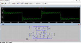
I've modified the amp some more. Also, I've plotted the data I got in a spreadsheet to have a better idea of power and efficiency. The efficiency is not great and it's possible to see that the worst dissipation is before (2*Vcc)/pi value (Vcc was 20/2 = 10V).
View attachment kamp.asc


View attachment kamp.asc
That's looking pretty good. I guess the next step would be to build a prototype and see how it behaves.
Efficiency is always going to be poor at low output levels for a linear amp, and that is where amps spend most of their time operating. Think of all the headphone amps we see running on say 30 volts and with 1 amp bias current, all to deliver a few 10's of milliwatts to a load. Now that's inefficiency
Efficiency is always going to be poor at low output levels for a linear amp, and that is where amps spend most of their time operating. Think of all the headphone amps we see running on say 30 volts and with 1 amp bias current, all to deliver a few 10's of milliwatts to a load. Now that's inefficiency
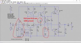
Add another filter capacitor parallel to R16. This filter to attenuate the noise generated by the 15V Zener.
Add in a resistor (47k to 100k) to the link from R16 to the input.
Adds pads into the trace in series with C6. You may need a resistance in there to shape up the response to fast signals.
You don't want excessively rolled off squarewaves due to a too big capacitor, but equally you don't want overshoot and some added resistance allows you to trim for an optimum response to fast signals.
Fast is the roll off of your input filter. Ah! You don't have one. Add in a pF (npo ceramic, or polypropylene) from Input Hot/Flow to Input Cold/Return
Last edited:
- Status
- This old topic is closed. If you want to reopen this topic, contact a moderator using the "Report Post" button.
- Home
- Amplifiers
- Solid State
- Tips on first amp design