Thanks for the circuit. However, in the simulator I am using, I found instability in the upper output stage. HOwever, that used 2N3440/2N5416 drivers as I did not have a model for the MJE340/MJE350.
I was not able to cure the oscillations yet, so I suspect it is the combination of frequency response of the driver and output combination. I've never seen the fT of the MJE340/MJE350. From other investigations I also suspect that a straight Darlington arrangement will work better.
I was not able to cure the oscillations yet, so I suspect it is the combination of frequency response of the driver and output combination. I've never seen the fT of the MJE340/MJE350. From other investigations I also suspect that a straight Darlington arrangement will work better.
I think that R36 (1k) should be connected to the base of Q1, other words to other side of R11. Connection to output is not helpful.Hi,
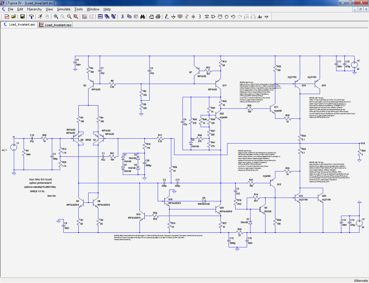
here is the schematic. It is more or less the schematic from D. Selfs Book APAD 6 Figure 10.12. The overload protection is ommited for clarity, as it is not used in the moment. In the simulation the rail sticking due to saturation is also visible, but not the oscillation. Tomorrow I will post some real screenshots from the oscilloscope.
View attachment 648952
Currently there are two grounds on the PCB - Input (input & feedback network) and power (decoupling Caps). Both grounds are connected by a separate wire to the star point on the PSU PCB. I will try to add a 10R resistor to input ground.
Best Regards,
Oskars
OK here's what I have found so far: the circuit does not show spurious oscillation on negative clipping using 2N3440/2N5416 drivers. With 1uH lead inductance in each of the main wires (+,-,spkr gnd and signal gnd) there is a spurious oscillation at positive clipping. If the drivers are MJE15030/MJ15031 there is oscillation at all points, not just clipping.
It can be suppressed with a Baker clamp on the CCS, and decoupling capacitors connected directly to ground. I used 100uF plus 1mF in series with 1 ohm resistors, to damp any ringing with the lead inductances.
It seems from this simulation exercise that the parasitics are related to the driver transistors, and lead inductances. I note that the circuit shows power supply suppression capacitors, so my guess is that they are physically too far from the output stage pair, or, that the ground connection is not ideal.
With the MJE drivers a 10 ohm resistor was needed in the emitters to suppress the oscillations too. So a combination of trying to reduce the loop gain in the output stage and reducing power supply line impedance at HF looks to be necessary.
Hate to say this ... but simulations look much more stable with conventional Darlington output stage (NPN/NPN and PNP/PNP). If you can't fix the oscillations with degen resistors, decoupling caps and a local earthy link resistor, and 100pF caps on the base-collectors of the drivers, suggest try swapping the output pair around. Will need to change the bias circuit to accommodate 4 Vbe's instead of 2, and use separate emitter resistors for the power transistors. Increasing the values to 0.33 ohms may be necessary to stabilise the quiescent current too, so it won't quite look like the original circuit.
BTW I would also use separate emitter resistors on the input diff pair to ensure equal currents, or you would need to match them quite accurately.
I believe Douglas Self would say that the CFP can be a tricky combination to stabilise.
BTW I would also use separate emitter resistors on the input diff pair to ensure equal currents, or you would need to match them quite accurately.
I believe Douglas Self would say that the CFP can be a tricky combination to stabilise.
In post 12 there was mention of testing using 15 volt and 32 volt rails - whereas in post 20 the attachment shows 42 volt rails - Miller capacitance in a common emitter amplifier (Vas) increases when the voltage seen at the collector is reduced.
If you are using 32 volt rails the compensation is not the same as for 42 volt rails.
If you are using 32 volt rails the compensation is not the same as for 42 volt rails.
I am not thinking about TMC so strictly arranged like in this example. Variations are possible, and in this example obviously necessary.This feedback arrangement is "transitional Miller compensation" or TMC.
I wonder if it could be oscillation around the Q16-Q24-Q15 loop? When over-driven and Q24 saturates, that loop would become quite slow.
What if, as an experiment, you opened up the collector of Q15, and then put a diode (1N4148) with anode to base of Q16, and cathode to collector of Q24? You might not want to end up that way, but it would give you some information.
If that worked, I might also try to raise R27 a bit...it says you can pull down about 6.8 times harder than you can pull up. Maybe with R27=33 Ohms, you'd still be ok, and you'd only be pulling down twice as hard as you're pulling up, which would be for more symmetrical limiting drive current, and as a side effect might keep the Q16-Q24-Q15 feedback loop happier if you decided to do that again.
Thanks for the circuit. However, in the simulator I am using, I found instability in the upper output stage. HOwever, that used 2N3440/2N5416 drivers as I did not have a model for the MJE340/MJE350.
I was not able to cure the oscillations yet, so I suspect it is the combination of frequency response of the driver and output combination. I've never seen the fT of the MJE340/MJE350. From other investigations I also suspect that a straight Darlington arrangement will work better.
For MJE340/MJE350 simulation models see - http://www.cordellaudio.com/book/Cordell-Models.txt
The schematic is the Load Invariant Design from D. Self.
As Conrad wrote, it must be something fundemantal. The oscillation seems to be independant from frequency (10 Hz to 20 kHz show the same behavior), load (4 or 8 Ohms, no load looks better) and supply voltage from +/-15 to +/- 32V behaves the same.
In all other situations the amp is stable. Square wave even at full load (until clipping starts) and 20kHz shows no sign of ringing.
Best Regards,
Oskars
It is not clear what supply rails you are using for your hardware. Are these plus and minus 42 volts as per Self's circuit and as shown in simulations of this or are these different.
Anyway, I copied the simulation attached to post 20 and adapted this for use with Bob Cordells transistor models - main changes are for small signal transistors MPSA types - these replaced by 2N5551 NPN and 2N5401 PNP.
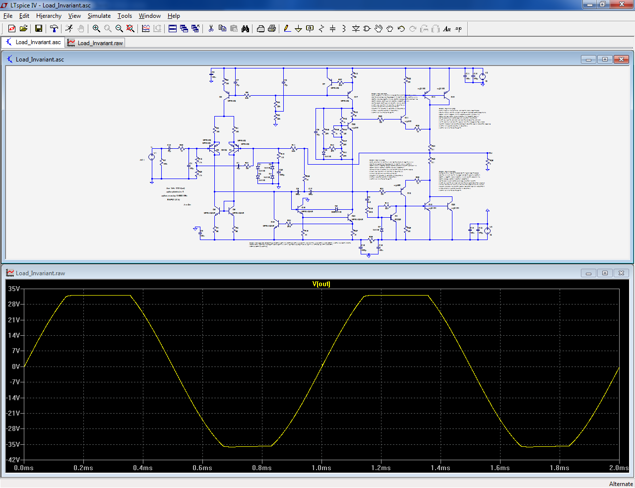
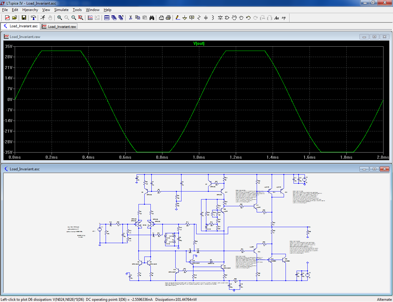
With added zobel network and series coil//resistor into 8R//2uF - at a glance the 1kHz sine wave looks normal, and the FFT and THD are OK below the level of clipping.
A 1.8 Volt input signal takes a bite size chunk out of the top and bottom of the sine wave cutting this back to 1.7 Volts gives a peak output voltage of 39 Volts which is pretty close to the rail voltage - I settled at 1.6 Volts in the end.
I will look at 20kHz sine and 10kHz square wave into 8R//2uF tomorrow.
The problem is caused by the utter unsuitability of the MJ2119x to the CFP configuration: even when they are not pushed into saturation, they store huge amounts of charge in their emitter junction, making the inversion extremely slow and difficult.
In addition, this also causes Xover artifacts because of the shoot-through current.
They would require a BE resistor of no more than a few ohms.
The problem could be solved with active accelerators, but it's probably not worth the complication:
Replacing the MJ's with just 2N3055's is even more effective, yet these are not exactly known for being fast:
An antisat diode at the VAS level also helps a little
Attachments
The emitter-base capacitance of the MJ21193/94 is indeed huge. ON Semi don't give the zero bias value, but at -2v they show about 5nF. It is not much different for the MJL3281A/MJL1302A if not worse. I agree using something like the 2N3055/MJ2955 might work. I've used them up to 70W but it is worth checking the BVceo. As I have commented before, several times, all the units I have measured from ON Semi and ST have worked to beyond 80V, but that is no guarantee, and the spec. still says 60V. As they are now epitaxial base devices, they are not bad, and much better than the old hometaxial RCA types. I have measured have fhfe's of 60kHz or thereabouts.
Having two MJ devices in parallel and only 100 ohm base resistors is troublesome. You could try reducing the base resistors to compensate, but the MJE340/350's could run out of steam pretty quickly, making a change of driver necessary, then maybe the VAS current needs increasing ...
Having two MJ devices in parallel and only 100 ohm base resistors is troublesome. You could try reducing the base resistors to compensate, but the MJE340/350's could run out of steam pretty quickly, making a change of driver necessary, then maybe the VAS current needs increasing ...
Dear all,
Thank you all for the detailed circuit analysis!!!
The output devices are mounted on a separate heatsink connected to the PCB by ~10cm long wires. The decoupling caps are directly at the connectors to the output devices. I tried already to increase the caps from 220uF to 1000uF on the PCB, but with no effect.
Currently I use a 2x32V@2x5A bench power supply to power the PCB. The power leads are ~50cm long. The supply is no name brand. I should check how the power rails looks like on oscilloscope... Maybe its part of the problem. The final PSU will have +/-42 V rails. That's where the 42V value in the LTSpice simulation come from.
I also switched from TCM (or output inclusive as D. Self calls it) to standart dominant pole scheme. With TCM it looked better. But until know I havent gone higher as 220p for all BC capacitance experiments... Maybe I should check it also with 330p.
The output devices must be in TO-3 package due to custom made casing. The side walls are used as heatsinks. At the moment I don't have any other types available. I will experiment around with all tips and hints you all proposed when I find time for it. If nothing helps, I will switch back to EF output stage. Since 5 years I use a selfbuilt minimalistic "blameless" amp using EF output with the same transistors. It's rock stable. The ongoing upgrade should add some more functions like short circuit protection, output relay etc. The main reason to switch to CFP output was the much smaller quiescient current. Unfortunatelly I didn't make the PCB universal for both output stage types
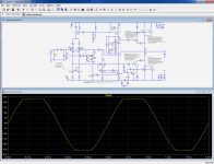
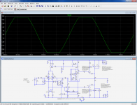
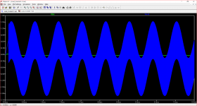
As promised, here comes the few measurements done @1kHz, ~20Vpeak and +/-32V supply.
Just before clipping:


Oscillations at light clipping:

Heavy clipping:

Thank you all for the detailed circuit analysis!!!
The output devices are mounted on a separate heatsink connected to the PCB by ~10cm long wires. The decoupling caps are directly at the connectors to the output devices. I tried already to increase the caps from 220uF to 1000uF on the PCB, but with no effect.
Currently I use a 2x32V@2x5A bench power supply to power the PCB. The power leads are ~50cm long. The supply is no name brand. I should check how the power rails looks like on oscilloscope... Maybe its part of the problem. The final PSU will have +/-42 V rails. That's where the 42V value in the LTSpice simulation come from.
I also switched from TCM (or output inclusive as D. Self calls it) to standart dominant pole scheme. With TCM it looked better. But until know I havent gone higher as 220p for all BC capacitance experiments... Maybe I should check it also with 330p.
The output devices must be in TO-3 package due to custom made casing. The side walls are used as heatsinks. At the moment I don't have any other types available. I will experiment around with all tips and hints you all proposed when I find time for it. If nothing helps, I will switch back to EF output stage. Since 5 years I use a selfbuilt minimalistic "blameless" amp using EF output with the same transistors. It's rock stable. The ongoing upgrade should add some more functions like short circuit protection, output relay etc. The main reason to switch to CFP output was the much smaller quiescient current. Unfortunatelly I didn't make the PCB universal for both output stage types
As promised, here comes the few measurements done @1kHz, ~20Vpeak and +/-32V supply.
Just before clipping:
Oscillations at light clipping:
Heavy clipping:
You picked it, the bench supply is a general purpose instrument. Just use it to get an indication your amplifier is working correctly.
Self avoids regulated supplies for power amplifiers - perhaps you can now see why. If you use 42 volt supply rails you could use his output inclusive compensation scheme with the capacitor values he prescribed.
You changed to standard compensation to improve matters with the amplifier in harness with the bench power supply - I think shackle might be a more appropriate word.
Having two MJ devices in parallel and only 100 ohm base resistors is troublesome. You could try reducing the base resistors to compensate, but the MJE340/350's could run out of steam pretty quickly, making a change of driver necessary, then maybe the VAS current needs increasing ...
In the past I have used these devices in simulations where these are a better fit than MJE15032/15033.
I may be stretching a point in the present case since there is no difference between these and MJE340/350 in the simulated the form of a 1kHz sine wave when the supply rails are set at 42 volts.
Reducing these to 32 volts does not adversely affect the amplifier with MJE340/MJE350 drivers - with input signal reduced to 0.9V to output 20 Volts peak.
If these are replaced with MJE15032/MJE15033 part of the sine wave trace becomes noticeably thicker so selecting these should not always be an automatic choice.
Hi All
I have had problems with Compound pairs (Unity gain lots of drive). I have used a BAKER CLAMP to stop the EB Storage (Turn Off). Try the simple approach to add a Schottky diode CB on the output stage has typically resolved the problems. Try a BAT41 is 100v 100ma. The VAS stage is not the problem.
Many time I force an offset and force a hard clip just to give a final layout test. Don’t forget to test low & high line testing.
I hope this will help resolve the problem.
In the past I have used these devices in simulations where these are a better fit than MJE15032/15033.
I may be stretching a point in the present case since there is no difference between these and MJE340/350 in the simulated the form of a 1kHz sine wave when the supply rails are set at 42 volts.
Reducing these to 32 volts does not adversely affect the amplifier with MJE340/MJE350 drivers - with input signal reduced to 0.9V to output 20 Volts peak.
If these are replaced with MJE15032/MJE15033 part of the sine wave trace becomes noticeably thicker so selecting these should not always be an automatic choice.
I have re-run the simulation with MJE15032/MJE15033 drivers where the supply rails are 42 Volts but with the input signal reduced to 0.9 Volt to output 20 Volts peak. The thickening of the trace when the supply rails were at 32 volts also show up under these circumstances - but not with MJE340/MJE350.
As the signal input is reduced the latter remain stable but things deteriorate with MJE15032/MJE15033. The attached screen capture shows the output with an input signal of 0.04 Volts
Attachments
- Status
- This old topic is closed. If you want to reopen this topic, contact a moderator using the "Report Post" button.
- Home
- Amplifiers
- Solid State
- I need a cure- oscillations at clipping