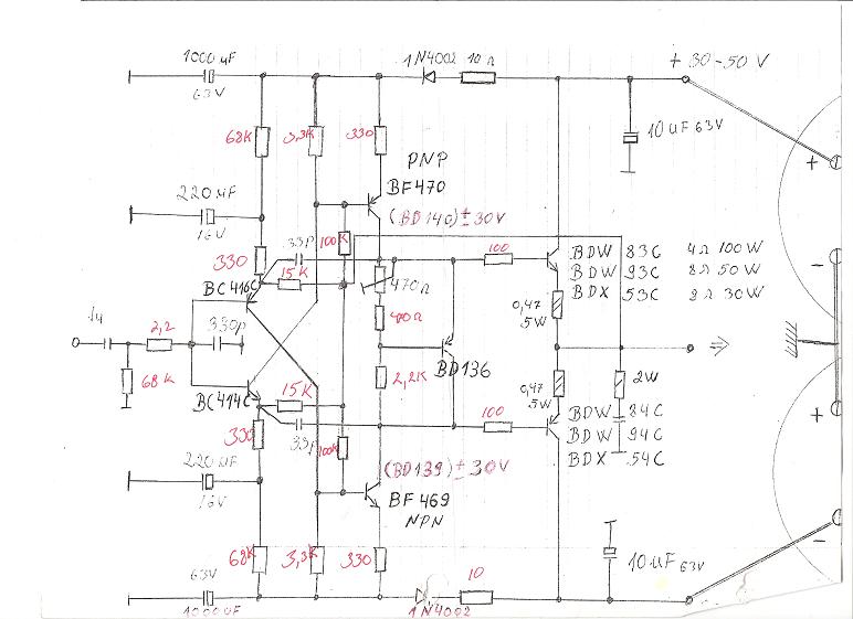
https://www.diyaudio.com/forums/attachments/solid-state/1001999d1638447744-cfh7-amp-cfh11_1v2_sch-pdfFollowing the naming convention for amps used in this thread and also first posted here, I am starting a new thread as this is not anything like an Apex design offshoot anymore:
100W Ultimate Fidelity Amplifier - Page 820 - diyAudio
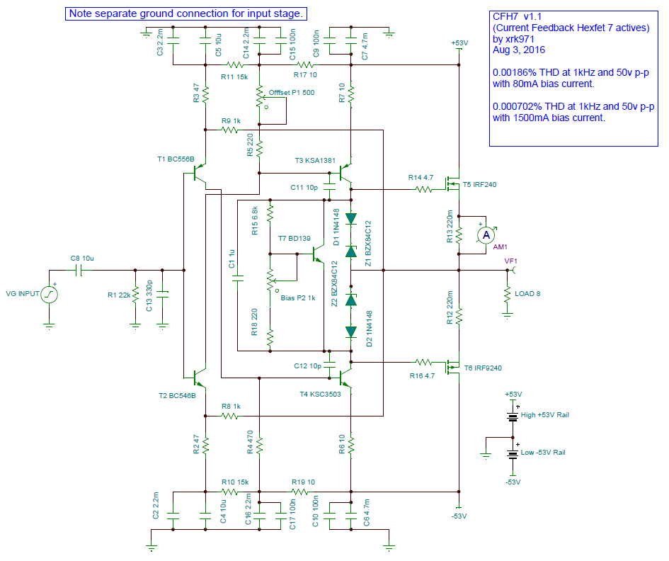
However, I think I will keep the standard naming convention that Apex Audio likes to use. So CFH7 stands for Current feedback HexFET with 7 active components. The amp arose out of the surprisingly successful FH9 and FH11/12 amp designs from the same thread, but with a current feedback topology that I believe was first used by Gaborbela as described here:
My first DIY amplifier 20 years a go - diyAudio
This same topology is also used in the very popular VSSA series of amps (VSSA, PeeCeeBee, FET-hex explendit, etc). My biggest inspiration for using the Gaborbela topology came after I built the amp described here:
VSSA Through-Hole Version by Jason - Page 86 - diyAudio
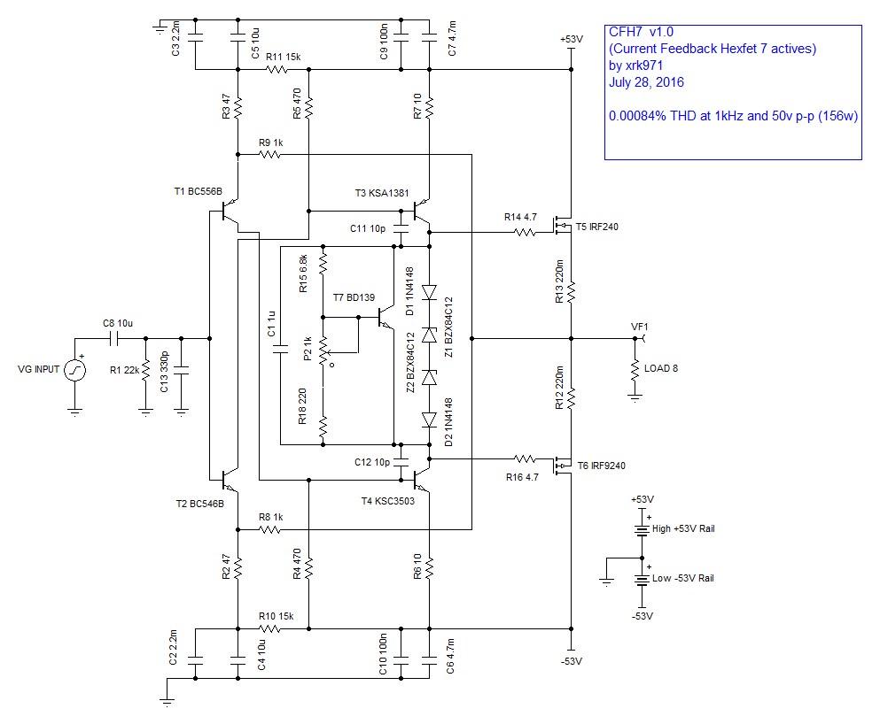
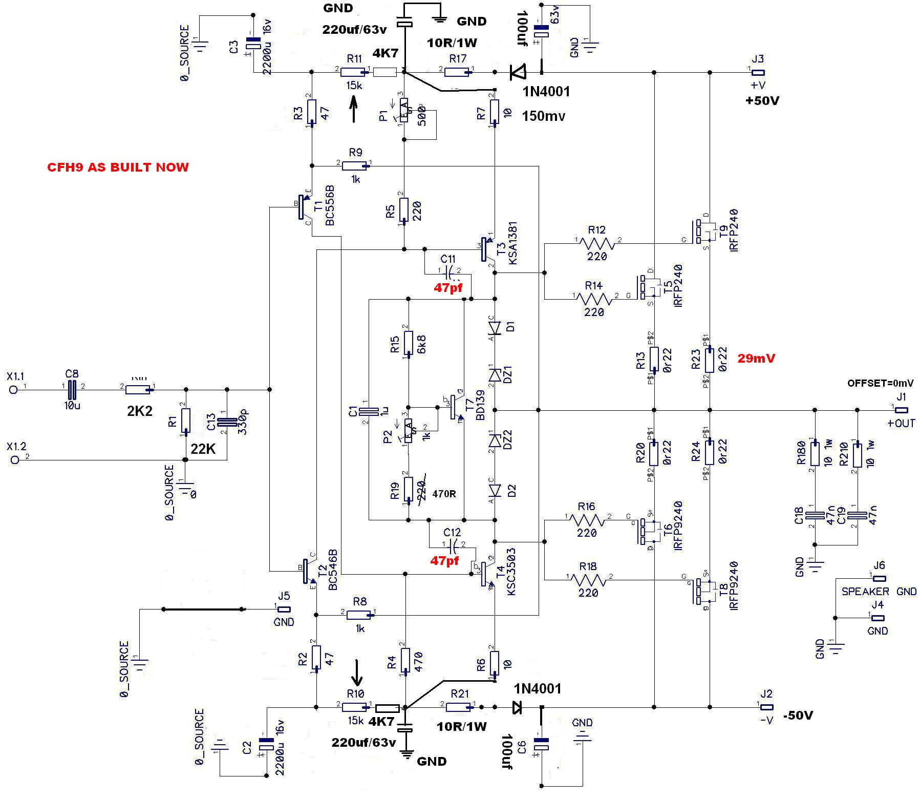
Now, I have applied the Gaborbela topology with the great sounding, popular and cost-effective IRFP240/9240 hexFETs, while reducing the number of active component parts count from the FH9, which has 9, to 7 transistors by elimination of two transistor CCS's. The simulations of this amp in TINA indicate a surprisingly good level of performance. The usual BD139 is still used for temperature compensation as a Vbe multiplier. Very large 4700uF rail caps are needed if you want the squarest square waves, but smaller 1000uF caps would probably sound just fine.
Here is the schematic:
And here are the simulated results:
1kHz sine wave at 50v p-p with 80mA quiescent bias current:

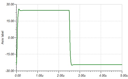
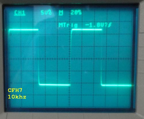
50kHz square wave:

200kHz square wave:
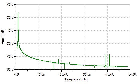
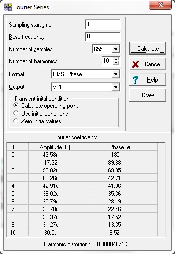
FFT spectrum at 1kHz:
HD components at 1kHz sine wave excitation:
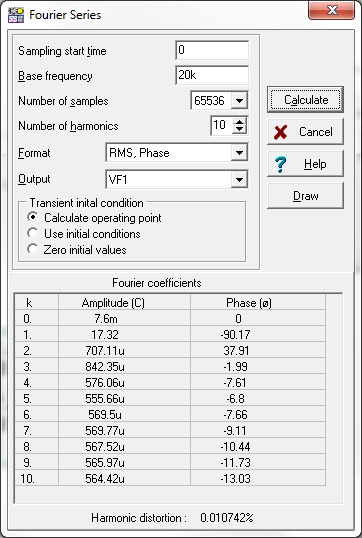
HD components at 20kHz sine wave excitation:
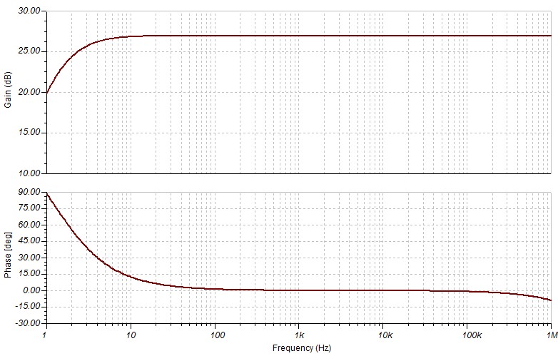
Gain and Phase as a function of frequency:
As you can see, the predicted HD of 0.00084% at 1kHz and the clean, sharp-edged square waves are very good indeed for a 7 active element amp that uses nothing exotic or special. Vishay hexFETs are available for under $1/ea, so this amp is literally under $5 to build. The bang for the buck on this amp is pretty much up there.
So, it's still in simulated schematic stage at this point and un-tested. I would welcome someone taking a crack at the layout for a Sprint/Gerber file and we can then test and listen.
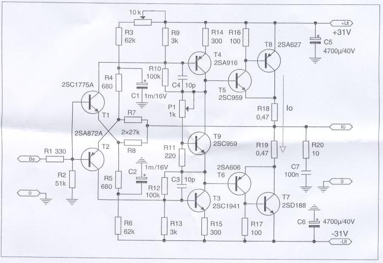
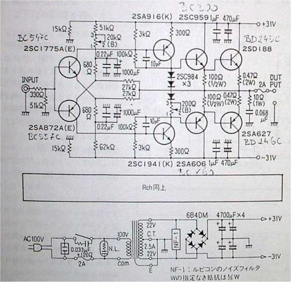
Edit Aug 3, 2016: several members have pointed out that this topology probably originated from Japan in the 1970's:
Version 1.1 schematic that Idefix will design layout for:
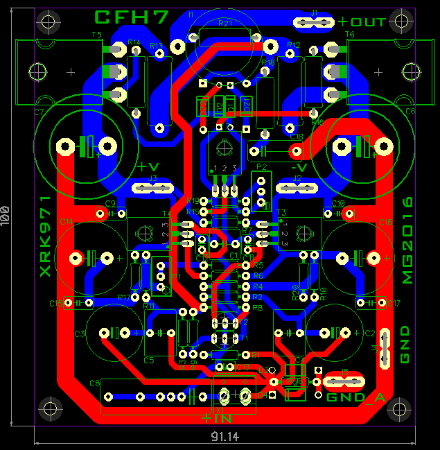
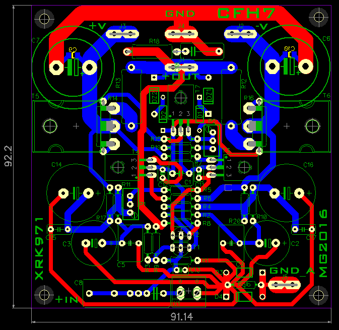
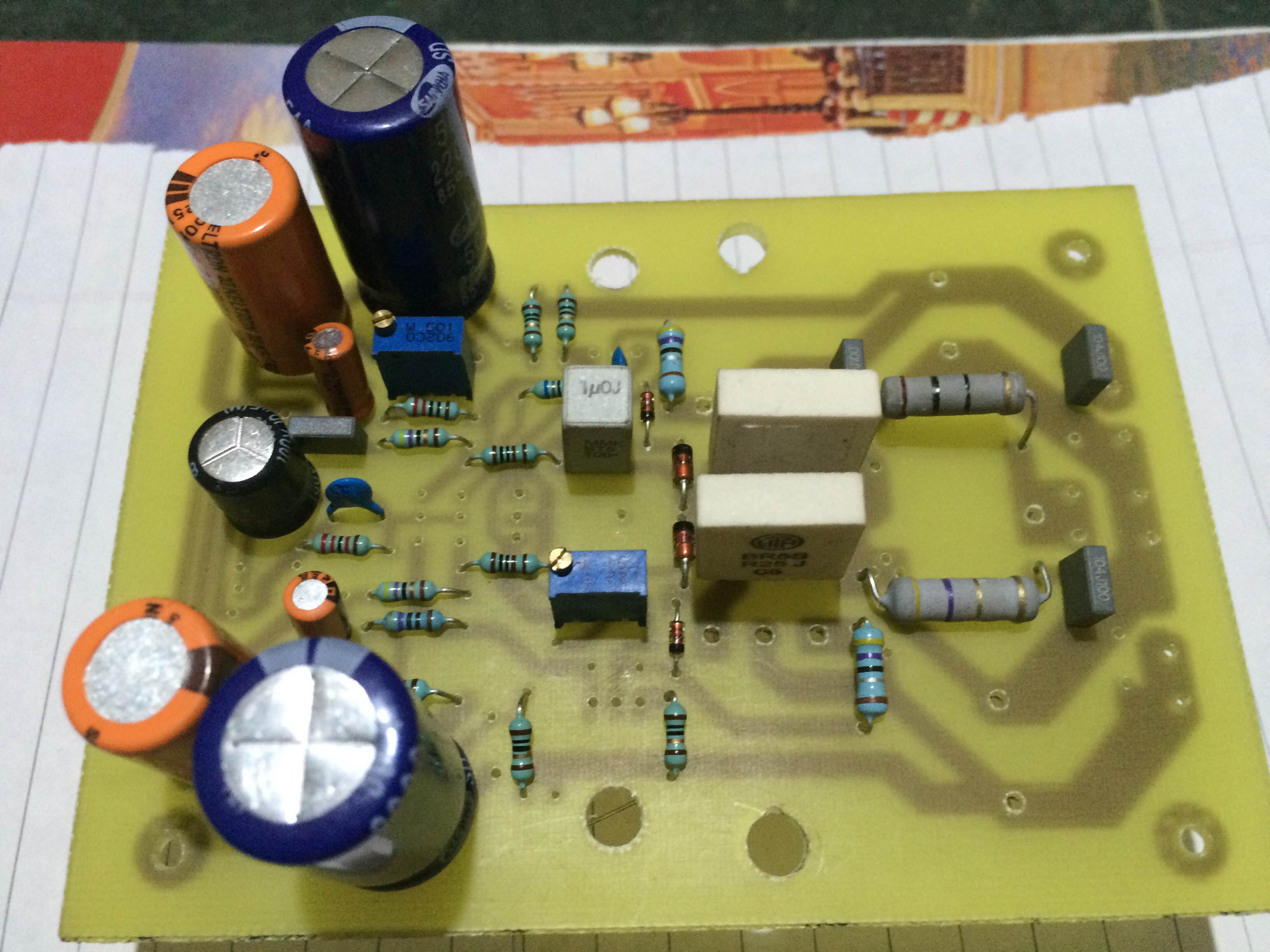
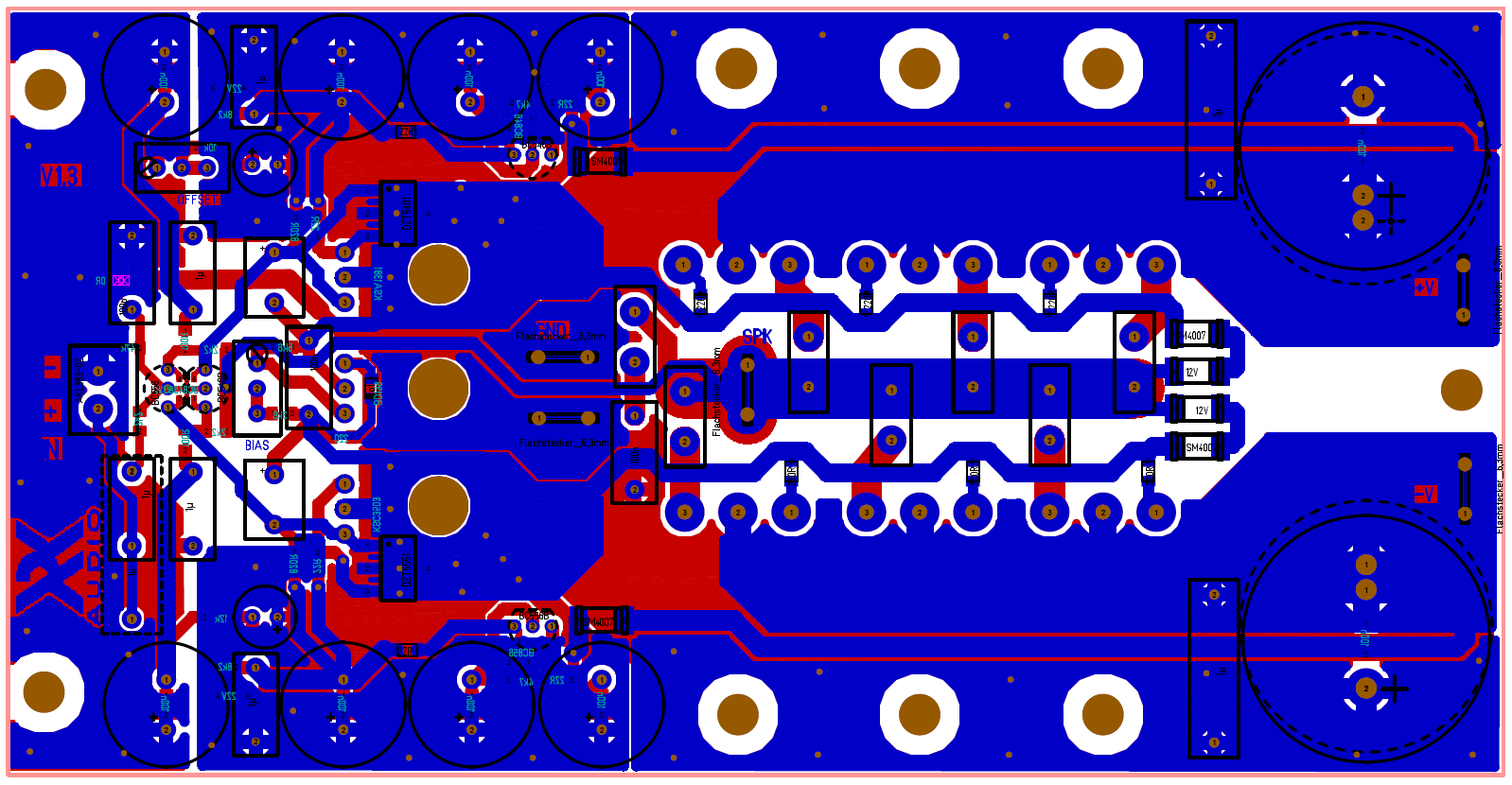
Update Aug. 7, 2016: Idefixes generated the new layout (with associated schematic for parts numbering):
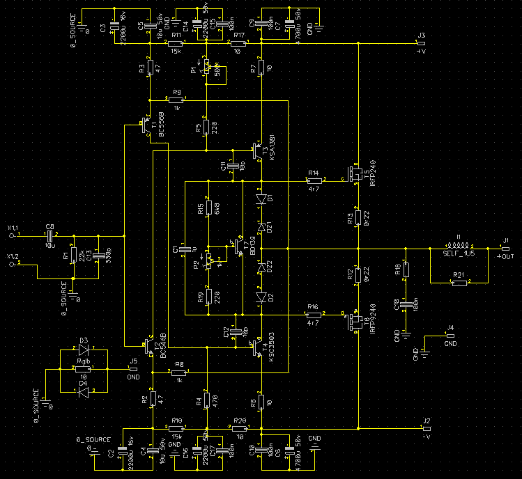
We are going to press with this layout - a masterpiece - great work Idefixes!
BOM for above amp:
http://www.diyaudio.com/forums/attachments/solid-state/572548d1475477936-cfh7-amp-cfh7-bom.txt
Edit: Aug 15, 2016 - Sonal Kunal has just developed a single sided layout - still not final but very cool looking.
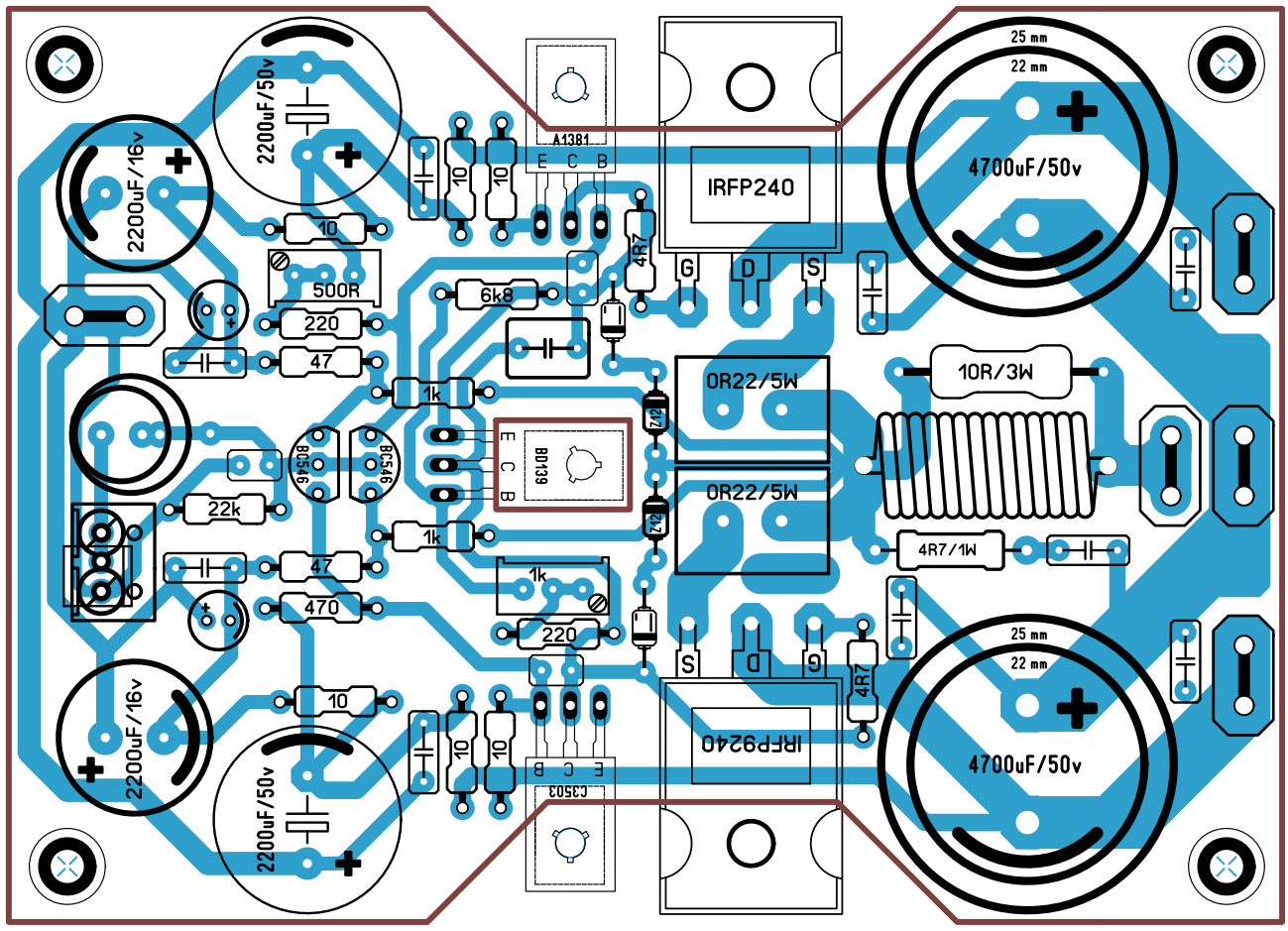
Edit: Aug. 16, 2106 - Latest layout from Sonal with no onboard inductor but 100mm max size
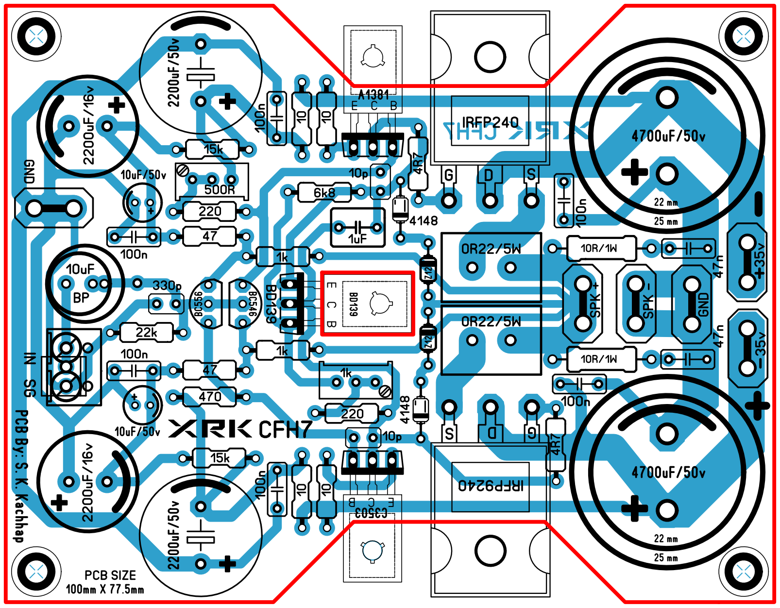
Edit: Aug. 17, 2016 - Idefixes has a beautiful new 2-layer layout that re-routes the ground bus to reduce RF spray onto the input stage:
So many layouts to try!
Still4given or Andrewlebon will probably be the first to reach first sound.
Andrewlebon in progress...
Still4given in progress...

I can't wait to see someone with a small waisted F1 car style board as Sonal has prescribed.
Edit Aug 19, 2016: Still4given had built and verified that Sonal's layout works but requires fixing wiring of Vbe multiplier as that has an error and also 4.7R gate stoppers are not enough to prevent oscillation. 100R seems to work there.
CFH7 Amp - Page 21 - diyAudio
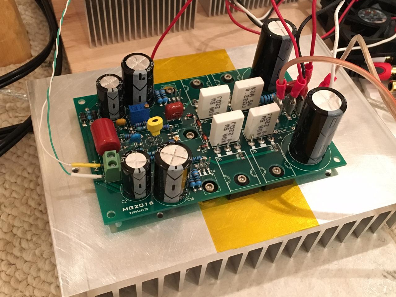
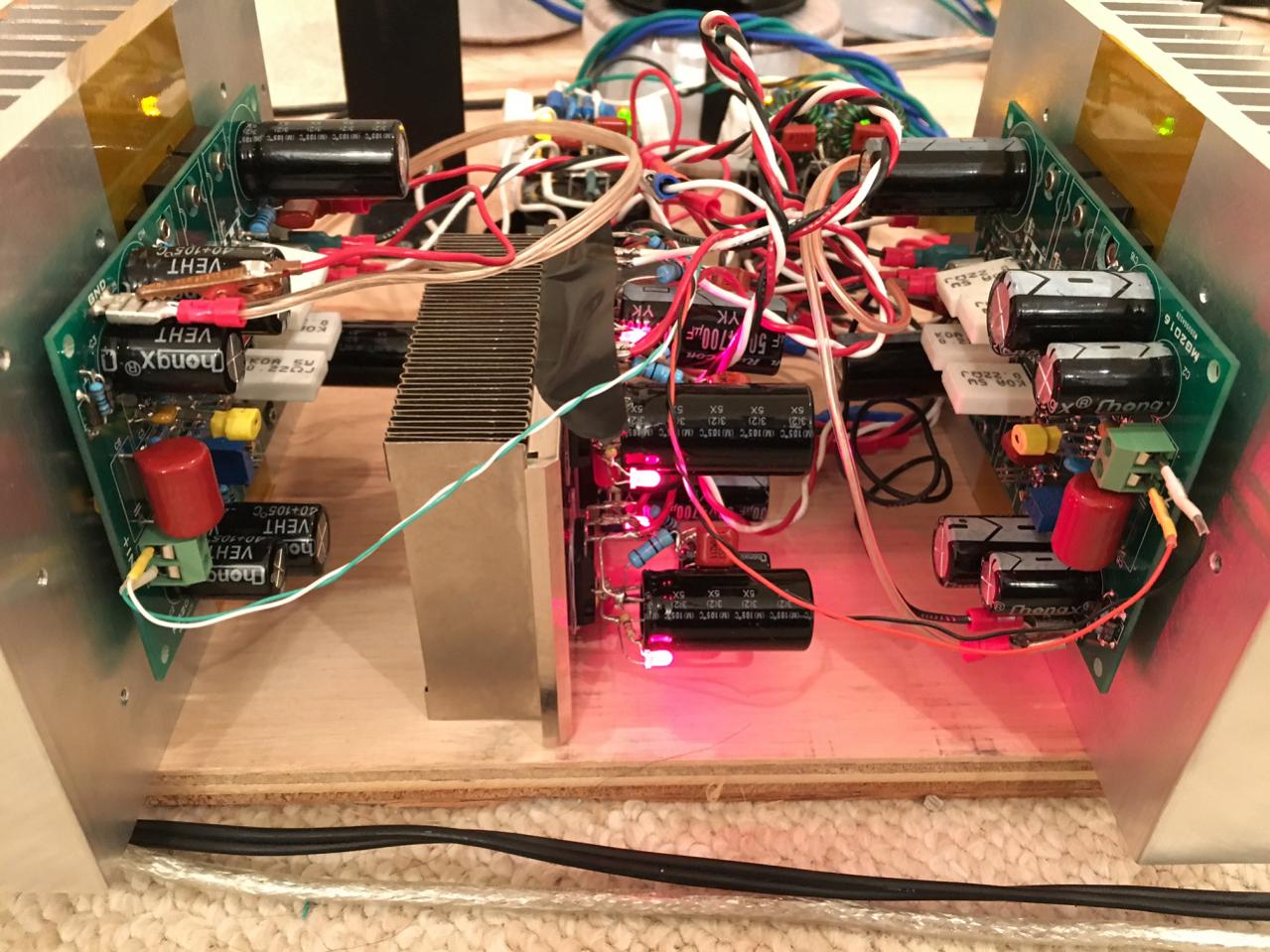
Here is a dual output pair version called CFH9:
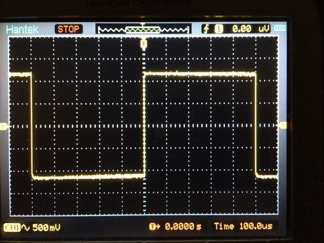
CFH9 works well - nice square wave:
CFH9 in stereo with Juma's Easy Peasy cap multiplier:
This is one of my top 3 amps.
Dec 16, 2016: Thanks to Thimios for finding grounding issue in design. Here is final mod to achieve very good PSRR and low THD. See post here
http://www.diyaudio.com/forums/solid-state/294834-cfh7-amp-82.html#post4920073
Edit Dec 5, 2021: saddevil has made a nice layout with some improvements in a cap Mx for the front end and one for the main outputs. This should have a really low noise background.
More info and Gerbers, here. Schematics here.
100W Ultimate Fidelity Amplifier - Page 820 - diyAudio
However, I think I will keep the standard naming convention that Apex Audio likes to use. So CFH7 stands for Current feedback HexFET with 7 active components. The amp arose out of the surprisingly successful FH9 and FH11/12 amp designs from the same thread, but with a current feedback topology that I believe was first used by Gaborbela as described here:
My first DIY amplifier 20 years a go - diyAudio
This same topology is also used in the very popular VSSA series of amps (VSSA, PeeCeeBee, FET-hex explendit, etc). My biggest inspiration for using the Gaborbela topology came after I built the amp described here:
VSSA Through-Hole Version by Jason - Page 86 - diyAudio
Now, I have applied the Gaborbela topology with the great sounding, popular and cost-effective IRFP240/9240 hexFETs, while reducing the number of active component parts count from the FH9, which has 9, to 7 transistors by elimination of two transistor CCS's. The simulations of this amp in TINA indicate a surprisingly good level of performance. The usual BD139 is still used for temperature compensation as a Vbe multiplier. Very large 4700uF rail caps are needed if you want the squarest square waves, but smaller 1000uF caps would probably sound just fine.
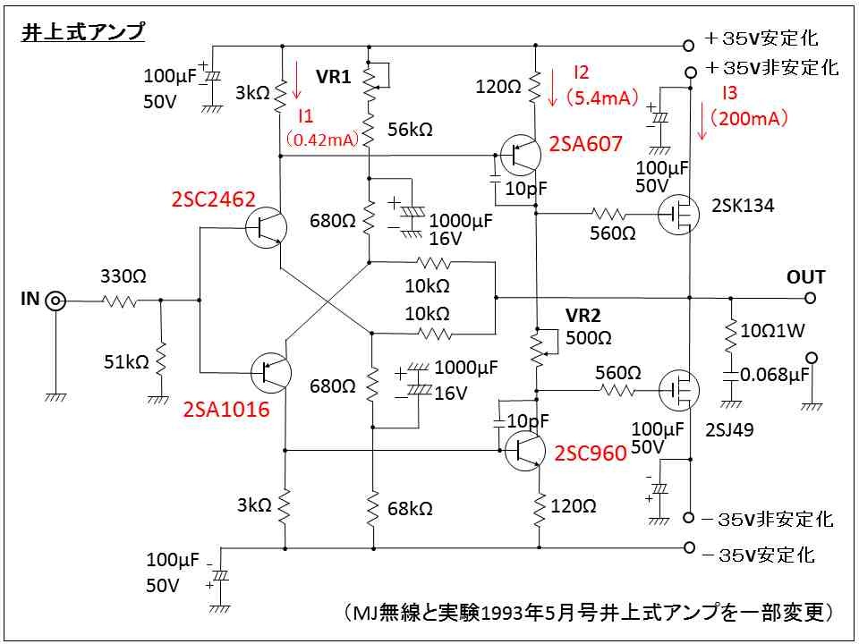
Here is the schematic:
And here are the simulated results:
1kHz sine wave at 50v p-p with 80mA quiescent bias current:
50kHz square wave:
200kHz square wave:
FFT spectrum at 1kHz:
HD components at 1kHz sine wave excitation:
HD components at 20kHz sine wave excitation:
Gain and Phase as a function of frequency:
As you can see, the predicted HD of 0.00084% at 1kHz and the clean, sharp-edged square waves are very good indeed for a 7 active element amp that uses nothing exotic or special. Vishay hexFETs are available for under $1/ea, so this amp is literally under $5 to build. The bang for the buck on this amp is pretty much up there.
So, it's still in simulated schematic stage at this point and un-tested. I would welcome someone taking a crack at the layout for a Sprint/Gerber file and we can then test and listen.
Edit Aug 3, 2016: several members have pointed out that this topology probably originated from Japan in the 1970's:
Version 1.1 schematic that Idefix will design layout for:
Update Aug. 7, 2016: Idefixes generated the new layout (with associated schematic for parts numbering):
We are going to press with this layout - a masterpiece - great work Idefixes!
BOM for above amp:
http://www.diyaudio.com/forums/attachments/solid-state/572548d1475477936-cfh7-amp-cfh7-bom.txt
Edit: Aug 15, 2016 - Sonal Kunal has just developed a single sided layout - still not final but very cool looking.
Edit: Aug. 16, 2106 - Latest layout from Sonal with no onboard inductor but 100mm max size
Edit: Aug. 17, 2016 - Idefixes has a beautiful new 2-layer layout that re-routes the ground bus to reduce RF spray onto the input stage:
So many layouts to try!
Still4given or Andrewlebon will probably be the first to reach first sound.
Andrewlebon in progress...
Still4given in progress...
I can't wait to see someone with a small waisted F1 car style board as Sonal has prescribed.
Edit Aug 19, 2016: Still4given had built and verified that Sonal's layout works but requires fixing wiring of Vbe multiplier as that has an error and also 4.7R gate stoppers are not enough to prevent oscillation. 100R seems to work there.
CFH7 Amp - Page 21 - diyAudio
Here is a dual output pair version called CFH9:
CFH9 works well - nice square wave:
CFH9 in stereo with Juma's Easy Peasy cap multiplier:
This is one of my top 3 amps.
Dec 16, 2016: Thanks to Thimios for finding grounding issue in design. Here is final mod to achieve very good PSRR and low THD. See post here
http://www.diyaudio.com/forums/solid-state/294834-cfh7-amp-82.html#post4920073
Edit Dec 5, 2021: saddevil has made a nice layout with some improvements in a cap Mx for the front end and one for the main outputs. This should have a really low noise background.
More info and Gerbers, here. Schematics here.
Last edited:
Hi xrk971,
-Chris
With those supply voltages, this amp has a lot of power available. However, your capacitance values for the power supply seem to be a factor of ten off, just wondering how to reconcile the capacitance values vs the apparent power output. If your rails are really bipolar 53 volts, what is your expected output power, and shouldn't you use another output pair for that level of power?Very large 4700uF rail caps are needed if you want the squarest square waves, but smaller 1000uF caps would probably sound just fine.
-Chris
Hi xrk971,
With those supply voltages, this amp has a lot of power available. However, your capacitance values for the power supply seem to be a factor of ten off, just wondering how to reconcile the capacitance values vs the apparent power output. If your rails are really bipolar 53 volts, what is your expected output power, and shouldn't you use another output pair for that level of power?
-Chris
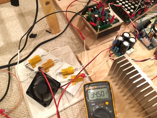
I was also warned of this with the FH9 but I tested it with 52v rails at 125w for 15min with no issues. The big 4700uF caps were chosen based on simulations of square waves having extra flat topped square waves at 50v P-P.
http://www.diyaudio.com/forums/soli...imate-fidelity-amplifier-790.html#post4768191
With FH9HV 34.5vac (48.7v p-p) into 10R load was no problem:
sure a typo, fliped (+ -) 53 mean (+ -) 35 ...
No, it's really 53. I tested FH9HV at 35 but it works fine at 53v. I assume same rails can be used for this amp.
Ok, I ll follow with interest, sure I can learn something valuable to apply to my similar but unsuccessful Darlington tryout
What happened with your circuit? Link?
There is a link missing between the two zener diodes and output.
Not sure the MOSFETs will survive a half-nasty real speaker at those rail voltages. 4 ohms is an accident waiting (not very long) to happen.
Also, the Vbe will be overcompensating. A LED in series with the emitter and a recalculation of the resistor values might solve this simply.
Not sure the MOSFETs will survive a half-nasty real speaker at those rail voltages. 4 ohms is an accident waiting (not very long) to happen.
Also, the Vbe will be overcompensating. A LED in series with the emitter and a recalculation of the resistor values might solve this simply.
Oh well, where to start... TIP 142-147 continue blowing well before reaching the + - 35VDC rail target, THD 1 watt 20Khz a mediocre 0.08%, FFT at 1W 20Khz shows a spray of harmonics, the odd ones clearly dominant throughout...
http://www.diyaudio.com/forums/solid-state/276360-darlington-vssa.html
Your s instead, shows excellent result from the start on.
http://www.diyaudio.com/forums/solid-state/276360-darlington-vssa.html
Your s instead, shows excellent result from the start on.
Hallo X.
Because i like simple Amps i must follow your new way VHEXSA and put other a bit behind.
Very nice simulation result- wow!- phase shifting looks very good.
What did you think about pairing 9140/240 like Borys- with good given reason- curves?
A fixed bias via 4148- borrowed from shaan?
If you picked any thinks up in your reflection?
Cheers Bangla.
Hallo X.
Because i like simple Amps i must follow your new way VHEXSA and put other a bit behind.
Very nice simulation result- wow!- phase shifting looks very good.
What did you think about pairing 9140/240 like Borys- with good given reason- curves?
A fixed bias via 4148- borrowed from shaan?
If you picked any thinks up in your reflection?
Cheers Bangla.
Z12 and 1n4148 string is from Apex amps (FX8, FH9, etc.) to protect gates on MOSFETs. Note I am missing connection from midpoint to amp output in schematic - need to add that.
Ilimzn,
Thanks for the note on missing link in between Zeners. Where did you think the LEDs need to go and why? I guess 4ohm would cause it to double the current. Double outputs like the FH12 would be better for sure.
In series with the emitter of the Vbe multiplier (bias spreader). This is because the actual voltage between gates will be around 8V, which is about 12x..13x Vbe. This also means the tempco is 12-13x that of a BJT, which is about 3-4x that of the MOSFETs. A green LED in series in the emitter, and a recalculation of the ratio of resistors to account fo the LED (~1.8V in addition to Vbe) will reduce the tempco to about 3x or so. Without this, the bias will overcompensate (instead of being constant with temperature, it will drop). This is not bad for reliability, but not for performance. Try simulating at different ambient temperatures and see how bias behaves.
the measurement units seem to be mixed up............with the FH9 but I tested it with 52v rails at 125w for 15min with no issues. The big 4700uF caps were chosen based on simulations of square waves...............
With FH9HV 34.5vac (48.7v p-p) into 10R load was no problem:
...............
http://www.diyaudio.com/forums/soli...hrough-hole-version-jason-86.html#post4781474
Here is the schematic:
[/IMG]
..............
A 100W into 8ohms amplifier will have 28.284Vac, = 40Vpk = 80Vpp driving the 8r0 load. This can usually be achieved from ~ ±50Vdc supply rails (at quiescent state). MosFETs in source follower mode will require slightly higher supply rails. ±53Vdc sounds about right to get to the 100W target.
Earlier I see 50Vpp and 156W being stated on ±53Vdc supplies. That can't be right. 156W into 8ohms is just not available from ±53Vdc.
50Vpp = 25Vpk = 17.68Vac and this equates to 39W into 8ohms.
The first quote shows
this too seems wrong.With FH9HV 34.5vac (48.7v p-p) into 10R load was no problem:
34.5Vac is 48.49Vpk = 97.58Vpp.
That is just about possible from a BJT or common source mosFETstage running on ±53Vdc, but seems just a bit too high.
34.5Vac into 10ohms is equivalent to 119W into 10ohms. That is too high for a mosFET source follower from ±53Vdc supplies.
Last edited:
Not a big deal- if you look with sharp eyes and comparing to other you can locate itNote I am missing connection from midpoint to amp output
The new ilimzn argues i understand a bit- Borys or Valery was given some clarification.
The bias current goes slow up and drift after warming up- down. A sensible technical
detail?
Also Andrews Calculation gives new points to learn/clear for me- not really understand
common source/source follower- next tiny step to learn.
Cheers Bangla.
the measurement units seem to be mixed up.
A 100W into 8ohms amplifier will have 28.284Vac, = 40Vpk = 80Vpp driving the 8r0 load. This can usually be achieved from ~ ±50Vdc supply rails (at quiescent state). MosFETs in source follower mode will require slightly higher supply rails. ±53Vdc sounds about right to get to the 100W target.
Earlier I see 50Vpp and 156W being stated on ±53Vdc supplies. That can't be right. 156W into 8ohms is just not available from ±53Vdc.
50Vpp = 25Vpk = 17.68Vac and this equates to 39W into 8ohms.
The first quote showsthis too seems wrong.
34.5Vac is 48.49Vpk = 97.58Vpp.
That is just about possible from a BJT or common source mosFETstage running on ±53Vdc, but seems just a bit too high.
34.5Vac into 10ohms is equivalent to 119W into 10ohms. That is too high for a mosFET source follower from ±53Vdc supplies.
When my DMM says 120vac when measuring wall outlet and I look at that in scope - are you saying it would have +169v and -169v peaks or 338v peak to peak? That doesn't sound right.
I do know that the DMM measured 34.5v AC in a 10ohm load. Power is voltage squared over resistance or 119w. How many volts peak to peak would that be on an o scope - so that I know how to interpret simulated Oscope traces to power ratings?
In series with the emitter of the Vbe multiplier (bias spreader). This is because the actual voltage between gates will be around 8V, which is about 12x..13x Vbe. This also means the tempco is 12-13x that of a BJT, which is about 3-4x that of the MOSFETs. A green LED in series in the emitter, and a recalculation of the ratio of resistors to account fo the LED (~1.8V in addition to Vbe) will reduce the tempco to about 3x or so. Without this, the bias will overcompensate (instead of being constant with temperature, it will drop). This is not bad for reliability, but not for performance. Try simulating at different ambient temperatures and see how bias behaves.
Hmmm... Several amps have been made with a BD139 Vbe follower like this and the bias current seems pretty stable. It might have to do with the large thermal mass the heatsink provides to slow down the overall time response. So it's like having a proportional integral derivative (PID) with high gain (P) and added mass for higher (I) so it all works out smooth and even. Perhaps sheer luck.
For a sinewave with nearly zero distortion:When my DMM says 120vac when measuring wall outlet and I look at that in scope - are you saying it would have +169v and -169v peaks or 338v peak to peak? That doesn't sound right.
I do know that the DMM measured 34.5v AC in a 10ohm load. Power is voltage squared over resistance or 119w. How many volts peak to peak would that be on an o scope - so that I know how to interpret simulated Oscope traces to power ratings?
Vac = Vpk/sqrt(2)
and Vpp = Vpk*2
So for sinewave 34.5Vac, you would have 48.79Vpk and that equals 97.58Vpp. The scope would show ~98Vpp
But the scope has the ground lead connected to mains Earth.
It measures from ground to output and that would be ~49V and shown as 49Vpp to which you need to apply the correction because you have actually measured Vpk of the sinewave even though the scope reading looks like 49Vpp.
But 97.58Vpk is not obtainable from ±53Vdc supply rails.
The rails sag when delivering big currents and the amplifier drops voltage across it's wiring and components.
CFP mosFET output drops very little voltage, roughly similar to BJT output stage.
Source follower output stage drops a lot of voltage and always gives much lower power than BJT from the same supply rail voltage.
Are you showing ±53Vdc as the sagged voltage at the output transistors when delivering full power? That would be roughly what a 40-0-40Vac transformer would give after sagging down from ~59, or 60Vdc.
Last edited:
- Home
- Amplifiers
- Solid State
- CFH7 Amp