Hi,
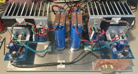
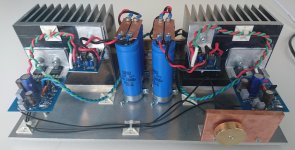
My first amplifier was the JLH class A design and I always thought it had a great sound and after I promised myself a long time ago I would build another one. As I wanted to play with some SiCdevices from Genesic devices it seemed like a great excuse. Anyway here is my effort, not quite the same, I changed the constant current part but it still has that wonderful class A sound. I have four ohm speakers,SEAS Acoustic Odin, and they worked fine with 2200uF, I dont know if the lack of damping somehow boosted the bass, but it sounded good anyway. There is an LTSpice sim and a KiCAD schematic and layout, the voltage regulator is just standard application note design. I went a bit "steam punk" on the build, so it has a WAF of zero, I will change the cable ties just as soon as I visit my local hardware shop or scrapyard and find something suitable. Be interested in feedback and I will try and help if anyone wants to build one, although its pretty straightforward.
My first amplifier was the JLH class A design and I always thought it had a great sound and after I promised myself a long time ago I would build another one. As I wanted to play with some SiCdevices from Genesic devices it seemed like a great excuse. Anyway here is my effort, not quite the same, I changed the constant current part but it still has that wonderful class A sound. I have four ohm speakers,SEAS Acoustic Odin, and they worked fine with 2200uF, I dont know if the lack of damping somehow boosted the bass, but it sounded good anyway. There is an LTSpice sim and a KiCAD schematic and layout, the voltage regulator is just standard application note design. I went a bit "steam punk" on the build, so it has a WAF of zero, I will change the cable ties just as soon as I visit my local hardware shop or scrapyard and find something suitable. Be interested in feedback and I will try and help if anyone wants to build one, although its pretty straightforward.
Attachments
Last edited:
Hi,
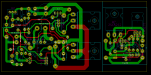
Here are the KiCad files I forgot to add yesterday for schematic and layout, I also added a potentiometer if people want to get the midpoint voltage more accurately than can be done by fixed resistance, a couple of hundred mV is fine by me but of course YMMV.
Here are the KiCad files I forgot to add yesterday for schematic and layout, I also added a potentiometer if people want to get the midpoint voltage more accurately than can be done by fixed resistance, a couple of hundred mV is fine by me but of course YMMV.
Attachments
These are very interesting devices, almost a bipolar but not quite. These are taken from the pdf from the manufacturer:
Drain – Source On Resistance [/B]
RDS(ON)
ID = 10 A, Tj = 25 °C 100milliohms
ID = 10 A, Tj = 150 °C 160milliohms
ID = 10 A, Tj = 175 °C 180milliohms
Gate – Source Saturation Voltage
VGS, SAT ID = 10A, ID/IG = 40, Tj = 25 °C
ID = 10A, ID/IG = 30, Tj = 175 °C
DC Current Gain hFE
VDS = 8V, ID = 10 A, Tj = 25 °C 100
VDS = 8V, ID = 10 A, Tj = 125 °C 65
VDS = 8V, ID = 10 A, Tj = 175 °C 58
They should deliver a very good saturation voltage Vds, far better than a bipolar which is little less than 0.2V for 8A. But why do they call it a gate when it is clearly passing hefty current, up to 1.3A on this device, more like a bipolar, and with a reducing beta as temperature increases, a bit like beta droop with a bipolar as current increases.
No reason why they would be able to run beautifully in the JLH, although driving a gate without any current on a standard mosfet seems to me to be more useful!
They are coming down in price, and they are very fast..... but are they faster than a big nmos?
Cheers,
Hugh
Last edited:
What does a SiC transistor sound like vs Si?
I havnt done a direct comparison to be honest, quite happy with how it sounds.
But why do they call it a gate when it is clearly passing hefty current, up to 1.3A on this device, more like a bipolar, and with a reducing beta as temperature increases, a bit like beta droop with a bipolar as current increases.
There was a guy that dropped into Pass Labs to flog off his wares, insisted it it's neither BJT nor FET but in summary never let on about anything except for the results.
In any case, people chase performance, the black magic can be explained in good time.
Last edited:
These are very interesting devices, almost a bipolar but not quite. These are taken from the pdf from the manufacturer:
Drain – Source On Resistance [/B]
RDS(ON)
ID = 10 A, Tj = 25 °C 100milliohms
ID = 10 A, Tj = 150 °C 160milliohms
ID = 10 A, Tj = 175 °C 180milliohms
Gate – Source Saturation Voltage
VGS, SAT ID = 10A, ID/IG = 40, Tj = 25 °C
ID = 10A, ID/IG = 30, Tj = 175 °C
DC Current Gain hFE
VDS = 8V, ID = 10 A, Tj = 25 °C 100
VDS = 8V, ID = 10 A, Tj = 125 °C 65
VDS = 8V, ID = 10 A, Tj = 175 °C 58
They should deliver a very good saturation voltage Vds, far better than a bipolar which is little less than 0.2V for 8A. But why do they call it a gate when it is clearly passing hefty current, up to 1.3A on this device, more like a bipolar, and with a reducing beta as temperature increases, a bit like beta droop with a bipolar as current increases.
No reason why they would be able to run beautifully in the JLH, although driving a gate without any current on a standard mosfet seems to me to be more useful!
They are coming down in price, and they are very fast..... but are they faster than a big nmos?
Cheers,
Hugh
I liked the fact that the gain is constant with current, i,e no bipolar gain droop but as you have pointed out it does drop with temperature but that is no bad thing as it means thermal runaway is less likely,
I did try a MOSFET, IRF240 for Q5 and Q4 but I could not get them to stop oscillating, I had the same problem with a complementary current dumping amplifier and could only get it to work with bipolars, I can only seem to get VMOSFETS working as source followers, in compound mode they always seem to oscillate for me, lateral ones are OK, if any one has any tips and tricks to get a transistor MOSFET Sziklai pair stable I would be very grateful.
The ones I used were these, which are a bit cheaper.
http://eu.mouser.com/ProductDetail/GeneSiC-Semiconductor/GA10JT12-247/?qs=%2fha2pyFaduiFuDr1S589GUz0CdGCyZs5c8NoisGKd4CUq4HmEtc6lQ%3d%3d
These would most likely work and are a lot cheaper at around six dollars each.
http://eu.mouser.com/ProductDetail/GeneSiC-Semiconductor/GA05JT12-247/?qs=sGAEpiMZZMv4z0HnGdrLjo8jrilP4RvOEd5%2fcR%2fm%252bmvekfQau%252b9qGg%3d%3d
Is it intentional that Q2 is a buffer stage rather than a voltage amplifier one.
Yes, there is not enough drive from the input transistor and if the next stage had amplification it would need an inverter which would add complexity. The JLH is a nice simple design.
Yes, there is not enough drive from the input transistor and if the next stage had amplification it would need an inverter which would add complexity. The JLH is a nice simple design.
I mentioned this as the design is purportedly based on Linsley-Hood's circuit with the BJT 's replaced by SiC's.
In the Linsley-Hood version the function of Q2 is to split the phase by inverting the input from the collector to base Q4 while preserving the phase input to Q5.
The output from the collector of latter will be inverted whether or not the connection from Q2 collector to base Q4 is extant.
The proof of whether this makes a difference would not be hard to accommodate. All that would be required is to provide optional jumper links for Q2 collector either to base Q4 or positive supply rail on the circuit board.
LTSpice shows a reduction in second harmonic of about 15dB and an increase in third harmonic of about 5dB with Q2 collector going to Q4, if there is no problem with stability on the test bench, then I will modify the PCB to accommodate both options.
LTSpice shows a reduction in second harmonic of about 15dB and an increase in third harmonic of about 5dB with Q2 collector going to Q4, if there is no problem with stability on the test bench, then I will modify the PCB to accommodate both options.
Stability in the Linsley-Hood version depends on the dominant pole being created by the slower 2N3055 outputs. Some builders have encountered instability having substituted 30 MHz fT devices.
Linsley-Hood's preferred stability method for more convention design was to bypass the output stage and the feedback resistor by a capacitor from Q2 collector connected directly to emitter Q1.
This establishes a permanent parallel feedback path at high frequencies. This gives R 2k7 in parallel with C at the choice of frequency turnover.
That should be based on giving precedence achieving an adequate stability margin - 45 degrees. You will have to experiment with this a bit. As a ball park starting point try 470 p.f.
Check to see there are no overshoots or ripple effects on square wave input of 10 kHz with 8R and 8R//2uF
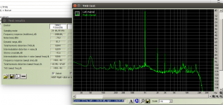
Hi - in the distortion plot in the first post it looks like you are using ubuntu. Can I ask what application you used to do the testing? - I'm lacking some good audio testing software under linux.
Thank you
Yep, it is indeed RMAA on WINE.
- Status
- This old topic is closed. If you want to reopen this topic, contact a moderator using the "Report Post" button.
- Home
- Amplifiers
- Solid State
- JLH Class A Silicon Carbide edition