I have seen some kinks around the knee of the rolloff during simulation,
The proportion of imagination to understanding here might be a bit high.
Christian
No kidding - sounds like a new dance craze.
Unfortunately or fortunately, but these circuitry was very advanced at the time when there were no complementary pairs of high current output transistors. Now we are provided with them and no longer need in this schematic.
the Quad triple was intended for constant quiescent current and that works well
because the junction of the power BJTs sense the junction temp "on the fly"
while sensing the temp of the heat sink has a considerable delay. insofar the idle current could sink too low to handle the next big impulse of the signal w/o increased cross over distortion.
The topology can be made symmetric.
It took me a moment...an EF has local feedback (I need a loop to remind me)
I only added the comment about the EF feedback at the last minute, as a reminder
") after you posted more or less simultaneously the next comment.
after you posted more or less simultaneously the next comment.The main point was that the CFP version has multiple feedback loops, from the emitter of the middle transistor (driver) back to the first (pre-driver) and also from the output transistor collector back to the driver emitter.
So one cut won't do it and we should analyse stability of each loop.
The overall response therefore may be an unreliable indicator of instability within an internal loop.
I don't yet have any feel for what to look out for in these situations, I chimed in partly to kick the idea around.
Secondly, you have parallel loops in the complementary halves.
I like an AC simulation but with a + or - 10 V offset in the input to see what each half looks like separately.
Maybe try that?
That article sounds like... I'd want to look at.
I haven't found a copy on the web, does your library have JAES?
AES E-Library Output Resistance and Intermodulation Distortion of Feedback Amplifiers
Dennis Feucht also has some informative stuff on EF instability that is easy to find on the web.
Best wishes
David
Last edited:
Secondly, you have parallel loops in the complementary halves.
I like an AC simulation but with a + or - 10 V offset in the input to see what each half looks like separately.
Maybe try that?
I haven't found a copy on the web, does your library have JAES?
AES E-Library Output Resistance and Intermodulation Distortion of Feedback Amplifiers
Dennis Feucht also has some informative stuff on EF instability that is easy to find on the web.
Yes, I'm definitely trying that! I was also going to step it through for load on each side.
I didn't find the article either but if it's full of matrix maths then I found a Doug Self summary, which was interesting. Apparently once the feedback in in place they have identical output impedances. Douglas did an interesting bit of schematic origami to show that they map onto each other. I'm not sure how that helps for the CFP though. I don't know if that means a CFP could be made identical to an EF. Probably not.
@Calvin Do you not think that the cutoff you found could be the result of too little current in the drivers. Perhaps you could do the sim with one my circuits which don't have the peak in response and are reasonably well balanced. Incidentally, the 3281/1302 output pair also work well with the ZTXes and BDs, giving a little bit more bandwidth with a < 1dB peak. I also want to see what the crossover region looks like with different Iq. I'm sure it will be as bad as any of the others.
All the best
Christian
PS. Can you give me a hint on how to do that Pulse test? Is it found under Voltage source and then you just changed one of those Earths to "in"?
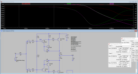
Hi!Interim circuit with ZTX pre drivers - reasonably balanced and with nice rolloff.
You used models of the transistors are far from perfect. I change them on the model from Cordell, and hump in frequency response vanished. Maybe, if you're using good models of transistors, many questions disappear as well, as the hump.
In addition, I remain of the opinion that the circuit design does not date, you're hoping for and not worth her time. This circuitry may be the only benefit: the experience and understanding, that no need to do so.
The peaking has come down here. It's very dependent on quiescent which I have kept around 100mA, but which changes with the components.
Looking at your "Darlington-in" arrangement, this is a medium power voltage gain and current gain stage in one - running a fair amount of highly fluctuating current through a 10 ohm collector load in each circuit half.
With regard to voltage gain stages operating in Class A, I have not seen a Darlington pair being used as the main voltage stage of a power amplifier.
When fluctuating heavy currents are drawn through the load resistor of a common emitter amplifier one has to consider possible effects such as Miller capacitance and Early effect (base width modulation) and how these might influence performance in the MHz range.
Do think it is highly fluctuating? I was working on the idea that 10R and the Vbe of the power transistor made up a current source and that was the problem with the earlier circuit with 47R that Calvin showed was going into cutoff. Someone also mentioned that a similar arrangement was on the Quad 303 and was quicker at mirroring the temperature and making sure that there was enough current. It's a nice idea.
I haven't seen any gain in there so far and the output is about 1dB down from the signal, but I'll have another look. I know there is a CFP arrangement with gain but the reports are that the distortion rises.
The Miller capacitance is what I'm trading of in fiddling around at the moment. I've got the bandwidth out to 5MHz (and have seen 7MHz, but that's hardly outstanding given the 30 or 40MHz components. Every time I try a more modern transistor as one of the drivers it reverts to peaking. The 653/753 is fine but it's interesting that a 5551 won't work, nor 3503/3601s.
Hi!
You used models of the transistors are far from perfect. I change them on the model from Cordell, and hump in frequency response vanished. Maybe, if you're using good models of transistors, many questions disappear as well, as the hump.
In addition, I remain of the opinion that the circuit design does not date, you're hoping for and not worth her time. This circuitry may be the only benefit: the experience and understanding, that no need to do so.
There is no hump in the frequency response with the ZTX drivers if you look further down the page. Are you using Cordell models or not? I don't think there is a Cordell model for the ZTX653/753.
As for distortion you haven't given any reason to say that this will be worse than an ordinary triple. I have shown you that the first component of distortion is 93.7dB down and you haven't answered that. The model for that is posted above.
In my asc-file specify the models directly in the title of the transistors. Of course, this model from Cordell.Are you using Cordell models or not?
I do not think that the work of a follower will strongly influence the type of these transistor, except, of course, quite obvious shortcomings, such as very large capacity Ccb or too low cutoff frequency current transfer. Because the input transistors operate in follower mode small-signal current, and the value of their Ccb is the problem, rather, VAS.I don't think there is a Cordell model for the ZTX653/753.
For me in this model all clear. With the same transistors, the same currents, Sziklai demonstrated the worst linearity. In practice, by the way, he also shows not the best results.As for distortion you haven't given any reason to say that this will be worse than an ordinary triple. I have shown you that the first component of distortion is 93.7dB down and you haven't answered that.
There is a way to know the distortion of the output stage of the amplifier directly. It is necessary in the model of PowerAmp to mark the entrance of the follower symbol, e.g. "1" or "3" is fine, and ask a Directive of the calculation of distortion for that point. The level difference of distortion between the input of the follower and its output is the required level of its own distortion in the mode with NFB and in normal conditions it works.
.
Yes, I'm definitely...
I look forward to see your results.
I didn't find the article either but if it's full of matrix maths... summary
It's been a while since I read it so I don't remember the exact content, but Dr Cherry does like a bit of maths
But he also explains what it all means, unlike many who do maths without much comprehension.
He replied to Self's summary in a later article, said Self missed some important points, so maybe better to pay attention to the abstract itself.
Best wishes
David
Looking at your "Darlington-in" arrangement, this is a medium power voltage gain and current gain stage in one -
I looked at this again and I very nearly missed something, which is that there is some feedback here that I really hadn't foreseen. (Yes, I was warned there might be.
) I was planning on doing something about this input biasing arrangement but hadn't thought it important but it really does need to have a better Vout/Vin.This is what happens in this circuit at n006, which is marked and is the base of the top pre-driver. We already have most of the rolloff defined at that point. I had initially glanced and thought that was just the ZTX defining it at the beginning, but no. That's the base. And not much else happens to the output until you get a decade further out.
So, from this, one can't see internal gain; though if there's a high impedance above a CE you can see how it would be happening. The input needs to be redone with a nice low impedance and then we might get a proper look at what is happening in the output stage by itself.
Here's the asc and the graph just for the record.
Attachments
Do think it is highly fluctuating? I was working on the idea that 10R and the Vbe of the power transistor made up a current source and that was the problem with the earlier circuit with 47R that Calvin showed was going into cutoff. Someone also mentioned that a similar arrangement was on the Quad 303 and was quicker at mirroring the temperature and making sure that there was enough current. It's a nice idea.
I haven't seen any gain in there so far and the output is about 1dB down from the signal, but I'll have another look. I know there is a CFP arrangement with gain but the reports are that the distortion rises.
The Miller capacitance is what I'm trading of in fiddling around at the moment. I've got the bandwidth out to 5MHz (and have seen 7MHz, but that's hardly outstanding given the 30 or 40MHz components. Every time I try a more modern transistor as one of the drivers it reverts to peaking. The 653/753 is fine but it's interesting that a 5551 won't work, nor 3503/3601s.
OK. Looking at the last point, consider that the collector of a transistor will be reverse biased in relation to the base giving rise to a capacitance within the diffusion - a form of opposites polarising rather than attracting. The capacitance developed is a function of the area of the transistor junction which is constant and inversely proportionate to the square root of the voltage applied to the collector.
The voltage drop across the 10 ohm resistor load shared by Q4 and Q5 will be more when more current is drawn when the collector to base capacitance will increase. I believe ZTX653/753 have the relatively high collector to base capacitance the alternatives tried may lack.
The voltage gain of a transistor is Gm multiplied by the load in k. ohms where as the Gm is roughly 40 mS per m.a. of collector current. The load will be that of the collector resistor and that presented by following stages.
I will leave you to reflect on the impact of reducing the original value of 47 ohms. I think it is worth taking a second look at the Crimson circuit in post 34 and possibly the Mission Cyrus 1 output triple.
Regarding biasing and cut off a strategy used in Darlington power devices is to incorporate a resistor from the base input of the first transistor to the base of the second - Q5 and Q4 in the circuit discussed. The small bypass current via a resistor of 4k ohm might help help recovery/ mitigate against cut off.
@mjona. It's 3.30am here and that is probably more than my little brain can manage in one hit. And are you sure that load isn't much higher than its nominal value? If it's a current source then it has a high impedance. The original Iq, said very much that it was a current source with it working out to exactly what you would get on a pocket calculator. It will vary with the Vbe of the power transistor, but not for some way beyond what we are doing so far.
I will work through what you are saying and I'm sure it's valuable.
I think I see what you are getting at and the two routes out of the pre-driver's emitter are going to vary the current through it, with the load very possibly varying with just one transistor between it and the loudspeaker's impedance. It's a hornet's nest. And one of the things I was hoping for is that it would present a nice high impedance to a VAS so that the gain wasn't modulated by the loudspeaker impedance curve. You are ahead of me on what's going on here but it is now nearly 4am (which probably calls for some Paul Simon, just to ease my brain). The input definitely needs redoing to see this at work but it might be worth presenting it with a real loudspeaker load to see if that really does turn up as a multiple at the input.
For 3 components there's an awful lot going on!
Edit PS. I did look at the hand drawn Crimson circuit earlier today, funnily enough. I will look again. I had no idea that the Cyrus did anything unusual so thanks for that tip. And thanks for your input too. Knowing how to simulate this stuff properly is not going to be easy. Already that input looks as though it was hiding stuff. Though that probably isn't the worst of it. G'night.
And are you sure that load isn't much higher than its nominal value? If it's a current source then it has a high impedance. The original Iq, said very much that it was a current source with it working out to exactly what you would get on a pocket calculator. It will vary with the Vbe of the power transistor, but not for some way beyond what we are doing so far.I will work through what you are saying and I'm sure it's valuable.
I think I see what you are getting at and the two routes out of the pre-driver's emitter are going to vary the current through it, with the load very possibly varying with just one transistor between it and the loudspeaker's impedance. It's a hornet's nest. And one of the things I was hoping for is that it would present a nice high impedance to a VAS so that the gain wasn't modulated by the loudspeaker impedance curve. You are ahead of me on what's going on here but it is now nearly 4am (which probably calls for some Paul Simon, just to ease my brain). The input definitely needs redoing to see this at work but it might be worth presenting it with a real loudspeaker load to see if that really does turn up as a multiple at the input.
For 3 components there's an awful lot going on!
Edit PS. I did look at the hand drawn Crimson circuit earlier today, funnily enough. I will look again. I had no idea that the Cyrus did anything unusual so thanks for that tip. And thanks for your input too. Knowing how to simulate this stuff properly is not going to be easy. Already that input looks as though it was hiding stuff. Though that probably isn't the worst of it. G'night.
Last edited:
... there is some feedback here that I really hadn't foreseen.
... how to simulate this stuff properly...
Are you familiar with the example in the LTspice library of how to check a feedback loop, the so-called "Tian probe"?
If not then it should be first on your list to study, there's plenty of examples in this forum.
If you already know it then I have implemented a few extensions and tools that may be useful.
I have posted the ASCs a while back, just search thru my posts with "Tian" in the text.
Some of those threads also contain discussions that really helped me understand.
Best wishes
David
Hi,
@Christian
in #64 You asked about increasing driver current.
That won´t help. While with the EF the output transistors basically supply for all the load and idle current alone, all the CFP transistors combine their currents.
So when the output transistor cuts off the driver transistor´s current is deformed from the sinusodial shape and THD of the higher harmonics shoots up.
Raising its idle current only raises the level where the deformation occurs and/or the driver cuts off also.
With the EF one only needs to ensure that the driver runs hot enough that it supplies for the output transistors base current.
jauu
Calvin
I did look at the hand drawn Crimson circuit earlier today,
I am the author fo this hand drawn schematics.
I did it in 1981, reserve engineering boards bought in a Glasgow shop.
Hi,
So when the output transistor cuts off the driver transistor´s current is deformed from the sinusodial shape and THD of the higher harmonics shoots up.
Raising its idle current only raises the level where the deformation occurs and/or the driver cuts off also.
With the EF one only needs to ensure that the driver runs hot enough that it supplies for the output transistors base current.
jauu
Calvin
I partially see where you are coming from but I see this as the driver(s) lending a helping hand. Do, btw, tell me where you think I am wrong. The first thing we do is get the available base current up to the same level as we would with an EF. In simple terms this should avoid cutoff in the first place.
If what was coming out of the output transistor was perfect then the driver transistor would have nothing to do beyond its function as a driver (in the same way as it would in an EF), though it may contribute pro rata since its emitter ends up in the same place. Only when it and the power transistor see something mistaken and Kirchoff doesn't add up does the feedback mechanism come into play. I see the driver's contribution as a good thing, able to make up for failings in the power transistor. If the power transistor cuts off then, sure, things will go a bit wild, but is that going to be worse than if the driver didn't try and correct it? I think the THD would be just as bad or worse. There could be a mechanism where the higher bandwidth of the driver gets in and makes mistakes that wouldn't be there with the slower transistor alone but that's deep speculation.
Have you tried this again, perhaps on my circuit which does have pretty identical currents top and bottom. There's a lot I need to do to that circuit like maybe putting a buffer at each input and getting rid of those 47k resistors, but repeating your test with the higher current available would surely be the first thing. Maybe I'm missing something, but could you show me that this problem is still happening?
All the best
Christian
Are you familiar with the example in the LTspice library of how to check a feedback loop, the so-called "Tian probe"?
No, that's new to me. It sounds very useful and I will have a look. I have never properly mastered the metaphysics of what's going on in feedback loops and how one knows what has and hasn't been corrected and I guess that's what you are getting at when you say the thread helped you understand things.
There's an awful lot to do here, and this is only on one topology so far! I haven't tried the sandwiched CFP yet not tried the option of splitting that 10R into two resistors. The thing is that I know a straightforward CFP worked very well in my regulator so I'm quite keen to stick with it if possible. I know it's a different application but it would be nice to have something that worked in both.
Thanks for that.
Christian
There's an awful lot to do here, and this is only on one topology so far!...
That's why I try to consider the problem from a top level perspective.
Kind of like you can analyse perpetual motion machines individually and try to study the forces in a mechanical scheme or the currents and potentials in an electrical one.
But it's quicker to use a concept like conservation of energy and rule schemes out en masse.
That's how the Cherry and Cambrell paper works, you don't need to know the details of the amp, if the loop gains are equal then the output impedances will be too. All you do is push the loop gain from one section to another.
Saves a lot of effort on unnecessary detailed calculations.
The master of this is R.D. Middlebrook, his stuff is available on the web, really excellent once one overcomes the initial unfamiliarity.
Best wishes
David
- Status
- This old topic is closed. If you want to reopen this topic, contact a moderator using the "Report Post" button.
- Home
- Amplifiers
- Solid State
- A three transistor compound pair?