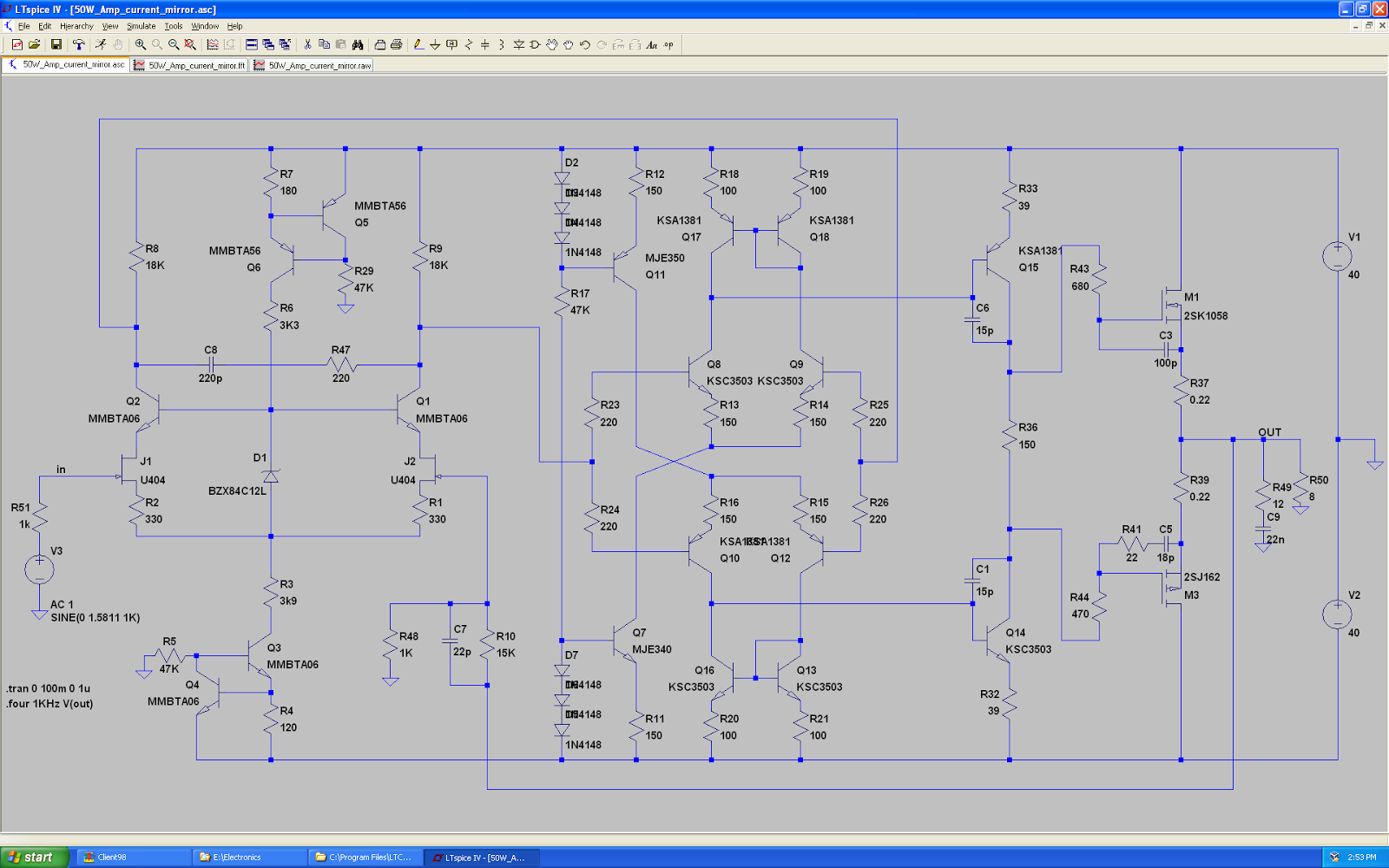
Bear in mind this is all simply simulation. I had to play with the compensation values a little to keep it from oscillating. This is one of the reasons I favour smd for these complex amps - fewer parasitics, so the reality is closer to the simulations and it makes for less frustration when it comes time to build it.
That's what I though you meant but wasn't sure. How do you set and stabilize the vas quiescent current with the mirrors in place? I suspect that the followers will reduce the hf distortion of the amp. Why not add some more output pairs - that will certainly reduce the distortion further.
Ah, thought you'd actually built it. So in real life you might find the vas quiescent current difficult to calculate and keep stable. A trick I've used in the past in similar cases is to place matched two terminal constant current loads between the collectors of Q15/Q17 and Q16/Q18.
Just so we're on the same page, here's my sim:
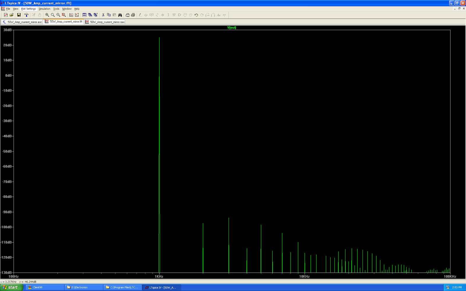
Fourier components of V(out)
DC component:0.000620999
Harmonic Frequency Fourier Normalized Phase Normalized
Number [Hz] Component Component [degree] Phase [deg]
1 1.000e+03 2.530e+01 1.000e+00 -0.11° 0.00°
2 2.000e+03 1.892e-05 7.478e-07 75.30° 75.42°
3 3.000e+03 2.918e-05 1.153e-06 -103.85° -103.73°
4 4.000e+03 2.716e-06 1.074e-07 164.72° 164.84°
5 5.000e+03 1.718e-05 6.793e-07 -95.39° -95.27°
6 6.000e+03 2.293e-06 9.063e-08 175.07° 175.19°
7 7.000e+03 9.412e-06 3.721e-07 -90.77° -90.66°
8 8.000e+03 2.108e-06 8.333e-08 -177.53° -177.41°
9 9.000e+03 4.871e-06 1.925e-07 -87.39° -87.28°
Total Harmonic Distortion: 0.000160%(0.000000%)
I added emitter degeneration to the mirrors. Your questions regarding drive current stability are very good - I think it's a case of "suck it and see", but I'm wondering if there's not a reasonable tradeoff to be made between gain and stability through degeneration.
Last edited:
The voltage at the Q10/Q16 collector junction isn't rigidly fixed, so the current through the Q14/Q15 vas transistors isn't well defined, which in turn means in real life its value would be a bit pot luck. You can solve that problem by inserting a two terminal constant current source ( two transistors, two leds, two resistors ) between the collector of either Q14 or Q15 and R36. I've used this trick with a two differential pair version of this topology ( ie the original non-symmetric Hitachi topology ) and it works well with no stability problems. The problem with applying it to your circuit is the further large increase in open loop gain, which might lead to stability problems, and necessitate some work with compensation networks. I'd be intrigued to see if it works however.
Hmm another thought. You might have trouble simulating the simple two terminal current source I mentioned. With ideal devices it should never self start, but in practice its 100% self starting and reliable. We might need to find a two terminal device that works in theory as well as practice.
But as you can see there are lots of solutions other than the one I used. I like stocchino's solution where he makes the vas one half of a current mirror to fix its operating point. Bob Cordells solution is neat too - uses a common mode signal to fix the operating point. I use the two terminal current source because its easy to undestand and you can fix the quiescent current precisely. This can be got to work and I'd like to see an updated/improved AEM6000. Not sure it'll sound any better but I'm dedicated to the pursuit of elegant circuits and the last ppm.
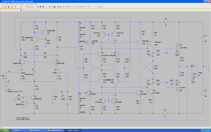
How's this look. I really wanted to preserve the symmetry. I figured I could add another current source/sink to the VAS to stabilise, separating out the two VAS transistors and tying the whole lot back to the current source/sink for the previous stage...
Fourier components of V(out)
DC component:0.000917462
Harmonic Frequency Fourier Normalized Phase Normalized
Number [Hz] Component Component [degree] Phase [deg]
1 1.000e+03 2.828e+01 1.000e+00 -0.04° 0.00°
2 2.000e+03 2.333e-05 8.249e-07 79.25° 79.28°
3 3.000e+03 2.341e-05 8.276e-07 -108.35° -108.31°
4 4.000e+03 2.028e-06 7.169e-08 144.80° 144.84°
5 5.000e+03 1.475e-05 5.214e-07 -95.81° -95.78°
6 6.000e+03 1.319e-06 4.663e-08 162.22° 162.25°
7 7.000e+03 8.930e-06 3.157e-07 -87.34° -87.30°
8 8.000e+03 1.163e-06 4.112e-08 178.86° 178.90°
9 9.000e+03 5.607e-06 1.982e-07 -81.01° -80.98°
Total Harmonic Distortion: 0.000134%(0.000000%)
Looks elegant, but still not sure if I can see any obvious mechanism that limits the current through Q14 and Q15. You could try checking the sensitivity of the simulation to small changes in things like the emitter resistors of Q14 and Q15. For simplicity and symmetry I'd personally go for the stochino scheme. Make each vas transistor one leg of a current mirror and use the other leg ( the one with the diode connected transistor ) to program the current. Put a 1k or so resistor between the bases of the mirror transistors to give some isolation. The stochino circuit is easy to find on the web, and in this forum, for reference. If you do it this way you know exactly what you're getting.
It's actually two independent sections. It's easier to see how it works if you cut it down the middle. Q14 is the VAS for the Q12/Q10 diffamp, and Q15 is the VAS for Q8/Q9.
Q19 is a current-source load for Q14, and Q20 is the current-sink load for Q15. In each case their current, and hence the VAS current, is set by the diode strings and their base resistors.
Finally R36 ties the two symmetrical halves together. It's value is chosen such that the current through it is a fraction of the VAS current for each side (you'll note it's now 620 ohms rather than 150 for 100mA bias). It also sets the final stage bias.
Biasing the final stage is a tad more complex with this arrangement than usual, as you've got to first ensure there's ample VAS current available by setting R32 & R33, then set R36 to an appropriate fraction.
Last edited:
As requested I played with the value of R32 (in isolation, as I figured this would be worst case):
39R: 8.46mA
33R: 8.49mA
47R: 8.45mA
Just for fun I chucked 100R in, and it was still 8.42mA. Interestingly there was a small decrease in distortion with 100R. It's allowing a little more voltage across the preceding stage current source/sink, which is a very good thing.
On the basis that I hadn't really played with any of the degeneration resistors despite changing bias currents, I went back and reduced the Q8,9,10,12 emitter resistors to 100R, and the J1,J2 source resistors to 220R, and promptly simulated 0.000088%, so I've hit my 1ppm target rather easily.
If I have missed something, and all is ok it might be time to think about a prototype. Be good if such a simple and elegant design were to hit 1ppm thd in reality. How does the stability of the latest version check out? Might be worth your while canvassing more learned heads than mine, just to be as certain as possible, before investing time in parts and solder.
I suspect, in real life, too that you'd need driver transistors for the mosfets if you wanted to keep the distortion to 1ppm levels at high frequencies. Incidentally what is the slew rate - I like fast amplifiers as well as elegant circuits - just for the intellectual fun of it.
a little food for thought to help avoid some potentially tough troubleshooting ...
there's a couple of current threads where the 2 bjt current source/sink made by Q5-Q6 and Q3-Q4 in suzyj's sch in post #30 might be prone to oscillate. sims won't necessarily show this. a suitable value base stopper resistor for the control transistor was suggested as an easy mitigation.
mlloyd1
there's a couple of current threads where the 2 bjt current source/sink made by Q5-Q6 and Q3-Q4 in suzyj's sch in post #30 might be prone to oscillate. sims won't necessarily show this. a suitable value base stopper resistor for the control transistor was suggested as an easy mitigation.
mlloyd1
a little food for thought to help avoid some potentially tough troubleshooting ...
there's a couple of current threads where the 2 bjt current source/sink made by Q5-Q6 and Q3-Q4 in suzyj's sch in post #30 might be prone to oscillate. sims won't necessarily show this. a suitable value base stopper resistor for the control transistor was suggested as an easy mitigation.
mlloyd1
Fascinating you say this, as I noticed this behaviour with one of my current amps. It's set up in my room at work, with a pair of little full-range speakers either side of my headboard, so I can listen at low volume of an evening without disturbing people in neighbouring rooms.
We recently installed a big solar-battery array to run the place (we're in the middle of nowhere in the desert, about 200km from the nearest grid connection), and it started driving me nuts, as when the solar inverters kick in at dawn it sounded like someone was running a motor mower next to my ears.
Turns out to be a weird low-frequency full-scale oscillation, which I guessed was caused by the current source/sink latching up somehow. Omitting the 22R resistors that isolated that stage from the supply cured it in practice, but I didn't really do much work to analyse the problem.
If I have missed something, and all is ok it might be time to think about a prototype. Be good if such a simple and elegant design were to hit 1ppm thd in reality. How does the stability of the latest version check out? Might be worth your while canvassing more learned heads than mine, just to be as certain as possible, before investing time in parts and solder.
First time ever I've heard anyone refer to an AEM6000 derived design as simple
")
I'm designing a layout as we speak.
Hello suzyj,
thanks again for this great design.
Sorry for 'stealing' this layout. Just a little more info, why i use this layout.
During my time at university in the 80ies, the first lateral Mosfet amps appeared here in Germany in the DIY scene.
There was a big discussion between the ELRAD design (POWER MOSFET 100 by David Tilbrook) and the ELEKTOR CRESCENDO. At this time i build the CRESCENDO and it's still running after a bigger modification a few years ago (The Crescendo).
Getting about ten pairs of genuine Hitachi 2SK1058/2SJ162 from a German DIY friend , i want to built the ELRAD design with these transistors, unfortunately it was based on TO-3 cases for the PowerMosfets and uses BF469/470 as drivers. Both were hard to find and progress in semiconductor development also took place in the past 30 years.
Checking the internet for actual amps ) using these laterals, i found your design including the PROTEL layout. I ordered 10 PCB from china for about €120 incl.fee, taxes shipment. 3 pairs i sold here at DIYAUDIO for price of costs (including all 0204 MELFs from Beyschlag, , the 2220 capacitors and the SST404 from LinearSystems). The new owners are located in England, Canada and Melbourne, Australia. Interesting one set finds it's way back home.
During Xmas time i will start to complete my PCBs, because my Hafler SE-100 (allfet preamp) waits new connection.
I hope you are not using this great design of yours.
Finally one question:
Which MJE340s/350s can be replaced by KSA1381/KSC3503, both E-grade?
Thanks again and Merry Xmas
 to Down Under from a winter cold
 Germany
Best regards
Günni
thanks again for this great design.
Sorry for 'stealing' this layout. Just a little more info, why i use this layout.
During my time at university in the 80ies, the first lateral Mosfet amps appeared here in Germany in the DIY scene.
There was a big discussion between the ELRAD design (POWER MOSFET 100 by David Tilbrook) and the ELEKTOR CRESCENDO. At this time i build the CRESCENDO and it's still running after a bigger modification a few years ago (The Crescendo).
Getting about ten pairs of genuine Hitachi 2SK1058/2SJ162 from a German DIY friend , i want to built the ELRAD design with these transistors, unfortunately it was based on TO-3 cases for the PowerMosfets and uses BF469/470 as drivers. Both were hard to find and progress in semiconductor development also took place in the past 30 years.
Checking the internet for actual amps ) using these laterals, i found your design including the PROTEL layout. I ordered 10 PCB from china for about €120 incl.fee, taxes shipment. 3 pairs i sold here at DIYAUDIO for price of costs (including all 0204 MELFs from Beyschlag, , the 2220 capacitors and the SST404 from LinearSystems). The new owners are located in England, Canada and Melbourne, Australia. Interesting one set finds it's way back home
.During Xmas time i will start to complete my PCBs, because my Hafler SE-100 (allfet preamp) waits new connection.
I hope you are not
using this great design of yours.Finally one question:
Which MJE340s/350s can be replaced by KSA1381/KSC3503, both E-grade?
Thanks again and Merry Xmas
Best regards
Günni
Last edited:
- Status
- This old topic is closed. If you want to reopen this topic, contact a moderator using the "Report Post" button.
- Home
- Amplifiers
- Solid State
- AEM 6000 ready to build