Well, after making a few gainclone gainclone amps for myself, I have a bunch of friends who want me to build them one, so I decided to make a pcb to simplify the build.
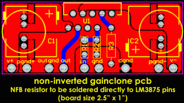
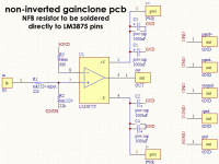
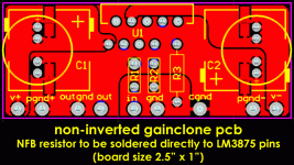
I am going to place the NFB resistor on the device pins to get the shortest signal path. For the capacitors, I want to try using some SMD Panasonic FK caps, in addition to the FC caps I have used before. I also added spacing for the BG caps.
Let me know if you have any comments/suggestions for the pcb.
--
Brian
Attachments
sek said:Hi Brian,
Negative Feedback?
Star Grounding?
Sebastian.
The NFB resistor is mounted off the pcb, directly to the LM3875 pins, as the schematic and pcb picture denotes.
As for the grounding, I had seperate ground planes for the signal ground, and for the power ground, and I join them together at the chassis ground pad on the pcb (CGND).
--
Brian
Sorry, Brian, I was editing my post while you replied!
That effectively means you've got your supply star ground on the board? Remember to ground everything on the board then. Of course you wouldn't be able to do stereo/multichannel applications with a single supply then...
Sebastian.
I join them together at the chassis ground pad on the pcb (CGND).
That effectively means you've got your supply star ground on the board? Remember to ground everything on the board then. Of course you wouldn't be able to do stereo/multichannel applications with a single supply then...
Sebastian.
sek said:Sorry, Brian, I was editing my post while you replied!
That effectively means you've got your supply star ground on the board? Remember to ground everything on the board then. Of course you wouldn't be able to do stereo/multichannel applications with a single supply then...
Sebastian.
I have my current setup with a single supply for two channels with no ground hum. What about this setup will cause problems?
Both channels will be going to the chassis ground.
--
Brian
If it works this way, then everything's fine. ")
Another one: I think your thermals are too narrow. You could easily implement some fuses here (e.g. at the V- pin of the chip).
Just another question: The blue lines are jumpered wires (e.g. underneath)? Can't you just route them on the board? There would be a possibility to keep proper ground-planing.
I'm just thinking about it... If you put the OUT pad right near the OUT pin of the chip and concentrated the grounding thing a little better (e.g. "real" star ground near the rectifier), you could move the caps together a little (e.g. in front of the chip). By doing so you could shorten the distance between the caps and the chip (it's stated to be important) and save board space (more prints per board sheet, more modules per heatsink, etc... At least Jeff wants 20, so efficiency is an issue).
Sebastian.
Another one: I think your thermals are too narrow. You could easily implement some fuses here (e.g. at the V- pin of the chip).
Just another question: The blue lines are jumpered wires (e.g. underneath)? Can't you just route them on the board? There would be a possibility to keep proper ground-planing.
I'm just thinking about it... If you put the OUT pad right near the OUT pin of the chip and concentrated the grounding thing a little better (e.g. "real" star ground near the rectifier), you could move the caps together a little (e.g. in front of the chip). By doing so you could shorten the distance between the caps and the chip (it's stated to be important) and save board space (more prints per board sheet, more modules per heatsink, etc... At least Jeff wants 20, so efficiency is an issue
).Sebastian.
sek said:If it works this way, then everything's fine.
Another one: I think your thermals are too narrow. You could easily implement some fuses here (e.g. at the V- pin of the chip).
Just another question: The blue lines are jumpered wires (e.g. underneath)? Can't you just route them on the board? There would be a possibility to keep proper ground-planing.
I'm just thinking about it... If you put the OUT pad right near the OUT pin of the chip and concentrated the grounding thing a little better (e.g. "real" star ground near the rectifier), you could move the caps together a little (e.g. in front of the chip). By doing so you could shorten the distance between the caps and the chip (it's stated to be important) and save board space (more prints per board sheet, more modules per heatsink, etc... At least Jeff wants 20, so efficiency is an issue
Sebastian.
I made the heat relief traces going to the pads larger, increasing to 30mils, and making a bigger one on the one going to the chip.
The blue lines are the traces on the bottom layer of the pcb.
I thought about putting the caps in front of the chip, but settled on this arrangement. The size of this board is already quite small... size the image to 2.5" x 1" on your screen (6.35cm x 2.54cm).
Thanks for your input. Here is the modified picture with thicker heat relief traces, and the bottom layer traces not shown.
--
Brian
Attachments
The blue lines are the traces on the bottom layer of the pcb.
You're planning to make it two-layered? Just because of three wires? That'll significantly increase cost and effort.
size the image to 2.5" x 1"
Do you have access to board material with multiples of 2.5" in a dimension? I tend to stick to either standards or what I've got.
OTOH, I'm only used to the European standard sizes anyway (e.g. about 2.35" x 4", 3"x4", 3.15"x4"). That would also mean that people copying your design outside the US couldn't keep up with your production efficiency.
Clever... Especially getting two-sided material in 2.5"... No, kidding... But while you're at it; what type of PS rectification and stabilization (if any) do you plan to use in conjunction with the board? Perhaps there's a chance that you can combine the effort to make the chipamp and the rectifier PCB (perhaps with central ground???) at the same time? Of course you would have to arrange the board sizes so that you can make single chipamp PCBs (in case you need more amps per rectifier than usual).
Sebastian.
sek said:
You're planning to make it two-layered? Just because of three wires? That'll significantly increase cost and effort.
Do you have access to board material with multiples of 2.5" in a dimension? I tend to stick to either standards or what I've got.
OTOH, I'm only used to the European standard sizes anyway (e.g. about 2.35" x 4", 3"x4", 3.15"x4"). That would also mean that people copying your design outside the US couldn't keep up with your production efficiency.
No, kidding... But while you're at it; what type of PS rectification and stabilization (if any) do you plan to use in conjunction with the board? Perhaps there's a chance that you can combine the effort to make the chipamp and the rectifier PCB (perhaps with central ground???) at the same time? Of course you would have to arrange the board sizes so that you can make single chipamp PCBs (in case you need more amps per rectifier than usual).
Sebastian.
I was just going to cram several on my next pcb order. It costs $33 each for a board, with a max size of 85 sq inches, double sided. I priced out boards a while back, and most places now use a dual layer process, so single layer boards would are about the same price as dual layer boards. As for the size, the board is small enough that the dimensions shouldn't matter that much.
I will work on a power supply board next.
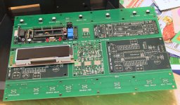
Here is a picture of a board from the last order, which I cut up to get my cdpro2 control board, dac board, buttons board and my Mini-Aleph board.
--
Brian
Attachments
That's fine
Then I'd say, fill the bottom layer with copper for grounding and the board fab with gainclones
Sebastian.
PS: I was just thinking of others to make those boards themselves, ease of transfer, etching, cutout, soldering, etc...
Have fun and supply some friends with some great gear!
Then I'd say, fill the bottom layer with copper for grounding and the board fab with gainclones
Sebastian.
PS: I was just thinking of others to make those boards themselves, ease of transfer, etching, cutout, soldering, etc...
Have fun and supply some friends with some great gear!
sek said:Hey Brian,
your group buy offer is getting lots of attention, great!
Have you actually tested the board?
It is a simple enough board that it should work fine. I ran a design rules check on the pcb layout, and it is functionally correct according to the schematic.
Do you have any concerns about it?
--
Brian
sek said:
Have you actually tested the board?
What is there to test, the "three wires"?
Peter Daniel said:
What is there to test, the "three wires"?
My sentiments exactly
--
Brian
Group Buy Boards
Hey Brian,
Just got my board and chips today. I must say I'm impressed with the quality of the board and timely delivery! I do have one small suggestion WRT the board design. With only a minor bit of re-routing of the traces for the rectifier section, the board could have more easily accomodated silicon rectifiers as well as diodes for those who would rather build the PS that way.
Thanks again for the great product and service!
Jimbo
- Status
- This old topic is closed. If you want to reopen this topic, contact a moderator using the "Report Post" button.
- Home
- Amplifiers
- Solid State
- Non-Inverted Gainclone PCB layout (LM3875)