Thanks Chris;
Your setup for matching is similar to what I came up with, except I use a zener reference and an op amp for the current source. I also put a 100K pot in parallel with one of the 10 ohm resistor loads, so that I could get the resistors matched to about 0.1 ohm. I didn't try to do that with the base resistors, and I still ended up with some offset. I'll explain how I dealt with that.
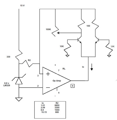
Instead of measuring collector voltage, I measured the difference between collector voltages on the two devices, using a millivolt meter. To the extent that there is any offset, caused by the circuit, it can be dealt with using a little more testing. Specifically, by swapping the transistors in the test jig.
One measurement will be V1=Vca+Vo-Vcb, and the other will be V2=Vca+Vo-Vcb, where Vca is the true collector voltage of Transistor a, and Vcb is the true collector voltage of transistor b. V1 and V2 are different, because any offset in the circuit will cause the voltage difference to be off by some amount Vo.
You can see that if I add the V1 and V2 measurements together, I get
V1+V2=(Vca+Vo-Vcb)+(Vca+Vo-Vcb)=(Vca-Vca)+(Vc-Vcb)+2Vo=2Vo, so I can determine the offset voltage for each test pair by measuring the transistors in one position and then in the other position, and adding the measurements, and dividing that by 2. I can then subtract the computed offset from one of the measured voltage differentials, and get the actual differential. Of course with ten hopefuls, this made for 90 measurements..
I measured the base voltages as well, but these were the same to below the resolution of my meter (0.05mV).
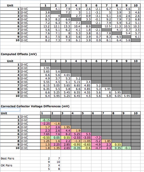
The results are shown below. I had a bunch of OK matches, a couple of very good matches, and one that was really terrible (device #6). The good pairs are matched to about 0.1 Mv.
I found that once in the jig, the devices settled down to a stable differential over about a 90 second period, so this took some time! The small plastic box over the test jig helped to stabilize the measurements too. I noticed that touching the case of either of the transistors caused about a 10 mV shift in the differential, so , yes, they are quite temperature sensitive!
Here is the matching table:
The top table has the raw measurements. Top half is the devices in one position, and the bottom is the devices in the other position.
The middle table is the result of the offset computation. You can see that the offset varied by about 2 mV. I actually went back and retested the first few pairs because after 40 minutes or so, the test jig itself had settled down. Those measurements were off by a couple of mV).
The bottom table are the corrected collector differentials. I went with pairs 2+7, and 9+10, since those were very close (0.1 mV).
I now have to invert this setup to do the P channel devices.
Cheers,
Scott
Your setup for matching is similar to what I came up with, except I use a zener reference and an op amp for the current source. I also put a 100K pot in parallel with one of the 10 ohm resistor loads, so that I could get the resistors matched to about 0.1 ohm. I didn't try to do that with the base resistors, and I still ended up with some offset. I'll explain how I dealt with that.
Instead of measuring collector voltage, I measured the difference between collector voltages on the two devices, using a millivolt meter. To the extent that there is any offset, caused by the circuit, it can be dealt with using a little more testing. Specifically, by swapping the transistors in the test jig.
One measurement will be V1=Vca+Vo-Vcb, and the other will be V2=Vca+Vo-Vcb, where Vca is the true collector voltage of Transistor a, and Vcb is the true collector voltage of transistor b. V1 and V2 are different, because any offset in the circuit will cause the voltage difference to be off by some amount Vo.
You can see that if I add the V1 and V2 measurements together, I get
V1+V2=(Vca+Vo-Vcb)+(Vca+Vo-Vcb)=(Vca-Vca)+(Vc-Vcb)+2Vo=2Vo, so I can determine the offset voltage for each test pair by measuring the transistors in one position and then in the other position, and adding the measurements, and dividing that by 2. I can then subtract the computed offset from one of the measured voltage differentials, and get the actual differential. Of course with ten hopefuls, this made for 90 measurements..
I measured the base voltages as well, but these were the same to below the resolution of my meter (0.05mV).
The results are shown below. I had a bunch of OK matches, a couple of very good matches, and one that was really terrible (device #6). The good pairs are matched to about 0.1 Mv.
I found that once in the jig, the devices settled down to a stable differential over about a 90 second period, so this took some time! The small plastic box over the test jig helped to stabilize the measurements too. I noticed that touching the case of either of the transistors caused about a 10 mV shift in the differential, so , yes, they are quite temperature sensitive!
Here is the matching table:
The top table has the raw measurements. Top half is the devices in one position, and the bottom is the devices in the other position.
The middle table is the result of the offset computation. You can see that the offset varied by about 2 mV. I actually went back and retested the first few pairs because after 40 minutes or so, the test jig itself had settled down. Those measurements were off by a couple of mV).
The bottom table are the corrected collector differentials. I went with pairs 2+7, and 9+10, since those were very close (0.1 mV).
I now have to invert this setup to do the P channel devices.
Cheers,
Scott
Last edited:
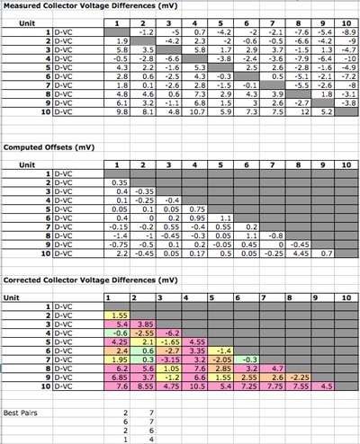
After some messing around, I ends dup basically just turning over the "load" section of the above diagram to test the p-channel devices. The devices don't care what the base potentials are, only the relative potentials, so it worked just as well driving them wight e same circuit, but with the collector loads tied to the op amp output, and the emitters tied to the input.
The results were somewhat more scattered than the n-channel results, but I did get a good set of pairs.
My various resistors and bits came today, and my replacement transistors shipped from China yesterday, so, I should be able to get this thing back together next week.
Cheers,
Scott
The results were somewhat more scattered than the n-channel results, but I did get a good set of pairs.
My various resistors and bits came today, and my replacement transistors shipped from China yesterday, so, I should be able to get this thing back together next week.
Cheers,
Scott
A correction to Post 21 above:
I wrote the voltage equations incorrectly..This SHOULD read:
One measurement will be V1=(Vca+Vo)-Vcb, and the other will be V2=(Vcb+Vo)-Vca, where Vca is the true collector voltage of Transistor a, and Vcb is the true collector voltage of transistor b. I have allocated the entire offset voltage to one side of the circuit, hence the terms (Vca+Vo) and (Vcb+Vo).
The differential voltages, V1 and V2, measured with the transistors in one position vs the other, are different, because any offset in the circuit will cause the voltage difference to be off by some amount Vo.
You can see that if I add the V1 and V2 measurements together, I get
V1+V2=[(Vca+Vo)-Vcb]+[(Vca+Vo)-Vcb]=(Vca-Vca)+(Vc-Vcb)+2Vo=2Vo....
Hi Scott,
I honestly don't know if that would work just right. Why not quickly wire up the PNP circuit and test one pair? Just as a sanity check.
What concerns me about your circuit is that the tail current must be very high impedance. One metric that determines how good a current source is, is its impedance (must be very high). That's why we don't like to see resistors as tail current sources. Your circuit is decidedly low impedance - very low in fact.
Maybe build a similar circuit to the one I have shown set for one current level. That simplifies things a lot. Then run your pairs through again. The parts that then forced to share current and there can be no deviation from that at all.
-Chris
Hi Scott,
I'm really interested in what you find. It would be fantastic if the transistors paired up the same. I do have my doubts. What current did you say you were running them at?
-Chris
I am running them at about 6 mA.
The transistors in your tester are obsolete. Do you have any equivalents?
Hi Scott,
Use any MJE part in a TO-126 case. The small 3mm LEDs will fit through the hole for better thermal coupling. Any current Japanese number in the same case will also work fine. Try 2SA1381 / KSA1381 and 2SC3503 / KSC3503 are currently available from the usual sources. Go for the highest gain parts you can get.
-Chris
OK, while I am waiting for a few transistors to arrive, I tested all of the resistors on the board.
I noticed that the manual says R114 and R145 are 499 ohms, but it also lists R114 as 33.2K.. I figured out that this is a typo, and it should be "R144, R145", not "R114, R145".
I found that the fusible resistor R157 was open, so I replaced it. I am not sure what a "fusible resistor" is, so I just put in a 10 ohm metal film resistor. I suspect this was a significant part of the problem with the board, since this resistor basically grounds the 220 uf Caps and their zeners, so they were basically operating with no ground reference. In circuit it tested out at 22 MOhms, and out of the circuit it was open (so the 22 Megs was the cap leakage).
So far, other than the oddball varistor thing I replaced with a KB362, and the improper zeners that I replaced with LM329s, I have found this one bad resistor, and two bad transistors. Two of the transistors had also been replaced with non-standard parts (Q110, and Q112).
I should get the bias tester transistors tomorrow, and will try retesting the darlington matched sets.
I have a couple more old stock transistors coming, a couple from China, and the Q110 from the UK..The internet is an amazing place!
Cheers,
Scott
Hi Scott,
Look at old stock transistors from China with great suspicion. You are further ahead substituting them with current transistors. While waiting for these, have a look at the current stock of parts from Digikey, Mouser and Newark. Just watch the lead pinout.
-Chris
Look at old stock transistors from China with great suspicion. You are further ahead substituting them with current transistors. While waiting for these, have a look at the current stock of parts from Digikey, Mouser and Newark. Just watch the lead pinout.
-Chris
After some research it looks like MPSA92/MPSA42 are reasonable replacements for 2SA1376 and 2SC3478.
These are also EOL, but Mouser has a lot of them..
The betas are a little on the low side, but are within spec.
Interesting that these higher voltage transistors were originally made for CRT TVs, and there is not much call for this sort of device nowadays..
These are also EOL, but Mouser has a lot of them..
The betas are a little on the low side, but are within spec.
Interesting that these higher voltage transistors were originally made for CRT TVs, and there is not much call for this sort of device nowadays..
Hi Scott,
If you buy the MPSW42 and MPSW92, assuming they have stock, you will upgrade the thermal properties of those parts to 1 watt collector dissipation.
Most transistors over 160 volts were designed for CRT TV applications. Don't forget that industrial uses also account for a large number of supplies being sold too.
-Chris
Mouser has several thousand of the MPSA 92/42 devices. These show a power dissipation between .625 and 1.5 watts, depending on temperature.
They do not have the MPSW devices.
These are in a TO92 package. They have many other similar higher power devices in TO-264 type flat packages with a heat sink mounting hole.
They do not have the MPSW devices.
These are in a TO92 package. They have many other similar higher power devices in TO-264 type flat packages with a heat sink mounting hole.
Hi Scott,
You should stay with the TO-92 case and the TO-126 case style has a different pin out. The "W" versions are TO-92M, meaning modified. The plastic case is larger but the pin out remains unchanged. The normal power rating is increased to 1 watt over the normal 625 mW rating for the TO-92 case style. Larger radiating surface, that's all.
When look at power ratings, look at the TA rating. 25° C is optimistic, an ambient temperature of 40° C is more realistic. 50° C if you are unlucky and don't have enough ventilation for the stuff in the box.
-Chris
Yeah, that's what I did.
Are there any pictures of the fan arrangement in the box (mine did not have that option).
I am assuming I could just hook up a small whisper fan and run it on reduced power to keep it quiet.
Maybe mount it in the top cover, just over the control board. It would then provide circulation throughout the interior of the housing, but it would keep the area around the control board at about 25 C.. (obviously not the junctions of the devices, but it would certainly help manage the heat...
It seems the original controlled fan would add a lot of complication for little actual benefit.
Hi Scott,
Yes, exactly. Run the whisper fan at reduced voltage using a resistor. If you put a N.O. thermal switch in parallel with the resistor, the fan can be made to turn on when the temperature exceeds your safety limit (normally 60 ~ 80 °C) depending on where the switch is mounted. Above the PCBs seems like a good choice for the actual fan. Any circulation can have a big effect on the running temperature of the amplifier.
I can't remember these units in detail, so I'll trust you on the comment on the original fan controller.
-Chris
The Adcom schematic shows a pretty complex fan control circuit. Way more complex than your good idea of a thermal on/off switch to run the fan full blast above some set temp.
The small rear housing piece that holds the control board (the u-shaped housing that sits between the heat sinks) has a bunch of cooling vents in the top. I am going to mount two fans 1 1/2 inches in diameter and 5/8 inch thick on standoffs below those vents. They will suck air in the vents and blow it over the board. The air will then circulate through the rest of the housing and out.
Today I replaced one of the speaker terminal posts (it had been soldered to, so the threads were all messed up), and the main power cord grommet (the cord was just snaked through the hole in the back....
Simple little things that differentiate a properly restored amp from a mistreated pile of junk...
Hi Scott,
I don't think any factory cooling kits were ever installed. I haven't really examined the circuitry for that since it wasn't used. It may have had some gradual speed up effect as the internal temperature increased to try and keep fan noise to a minimum. My thoughts on that matter are pretty simple. If you are driving the amp that hard, you can't hear a fan roaring away in the case. Besides, its now a choice. Dead amp, or some noise because you are running it beyond reasonable levels.
I think that the greatest benefit comes from a fan running at reduced CFM constantly. That will drop the temperature quite a bit. However, you should always work with natural convection currents rather than against them. Also, consider using some kind of filter across the air inlet. Otherwise you can demonstrate just how efficiently these amps can be made into a vacuum cleaner. The dust is suspended in the rapidly moving air, and when that air slows down, it drops anything that was suspended in it. Voila! An air cleaner. You are better of by pressurizing the enclosure than evacuating it. Positive pressure tends to blow dust out from every nook and cranny. Evacuating the enclosure reverses the process and collects everything instead, jamming it into every nook and cranny.
I haven't noticed any natural locations for a fan with these amps. I haven't looked for any either.
-Chris
My 585 has the stock fan.they are rare but do exist.by the way, anatech ,your contributions have been valuable, i restored mine with what i have been been reading in this forum.needs some more work done to it but i am getting there.fan position is below the top cover of the amp.Hi Scott,
I don't think any factory cooling kits were ever installed. I haven't really examined the circuitry for that since it wasn't used. It may have had some gradual speed up effect as the internal temperature increased to try and keep fan noise to a minimum. My thoughts on that matter are pretty simple. If you are driving the amp that hard, you can't hear a fan roaring away in the case. Besides, its now a choice. Dead amp, or some noise because you are running it beyond reasonable levels.
I think that the greatest benefit comes from a fan running at reduced CFM constantly. That will drop the temperature quite a bit. However, you should always work with natural convection currents rather than against them. Also, consider using some kind of filter across the air inlet. Otherwise you can demonstrate just how efficiently these amps can be made into a vacuum cleaner. The dust is suspended in the rapidly moving air, and when that air slows down, it drops anything that was suspended in it. Voila! An air cleaner. You are better of by pressurizing the enclosure than evacuating it. Positive pressure tends to blow dust out from every nook and cranny. Evacuating the enclosure reverses the process and collects everything instead, jamming it into every nook and cranny.
I haven't noticed any natural locations for a fan with these amps. I haven't looked for any either.
-Chris
Cheers
- Home
- Amplifiers
- Solid State
- Yet Another Adcom GFA-565 Thread