Whoa, thanks for all the responses! Unfortunately, due to time zone issues it will be some time before I can get home to work on this, but let me go through this here...
The real amp. These particular FETS seem to have a Vt of about 3.5V. I pretty much determined the needed resistor values empirically.
Interesting suggestion. C23 was specifically added because I found that it helped to prevent oscillation in my breadboard prototype. I may try removing C20. Adding a Miller cap at Q9 also seems like a good idea.
Really? Maybe I should switch to LTSpice then... I am surprised that your simulation is able to replicate the oscillation when mine does not. For me, Pspice simulations have NEVER been able to predict oscillations correctly, even in some instances where I was intentionally designing an oscillator.
As for adding "gate stoppers", I admit that am not familiar with the term. I will research this further. (I apologize, it seems that now the truth comes out that I am an utter novice at this and my self-taught knowledge base is full of holes).
Whoa, thank you for this detailed analysis work!
Hmm. Again, it seems my main area I need to improve is on the simulation side, and this would have exposed a lot of the issues I am having now much sooner. This analysis of gain and phase margins seems particularly useful, and is not something I had done when designing this.
Actually, I did find out about the thermal runaway issue first hand during testing. I have been using a small cooling fan to mitigate this, but I do realize that this is bad design practice on my part.
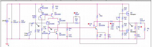
What, if any, is the significance of the Red/Green circling on the schematic for that high power spreader/power stage?
Also, correct me if I am wrong, but the N-channel FET I am using is IRF540N, which actually seems to be a different part from IRF540 as far as I can tell from the datasheets. your comments on matching the capacitances makes a lot of sense, though. I had chosen the parts merely because their transconductance characteristics were similar, even though IRF4905 has a much higher input/output capacitance then IRF540N.
Unfortunately, as I have already soldered components to a board, I will likely only make the bare minimum changes to get this working, or scrap the project completely and start over using what I have learned from everyone's comments.
That redesign of the biasing structure looks interesting, and I can see how it might be more stable. my current biasing structure is a holdover from some of my much earlier design prototypes that had no feedback between stages at all, basically just two fixed-gain class A stages followed by that power stage, each with their own bias resistors. I eventually rejected these designs as they had poor linearity (my original design goal for this project was a modest goal of <1% THD), and went with a more controlled design using the long-tailed pair seen in my current design. Also, I presume that the Set_Bias resistor should be a trimmer of some kind in an actual layout?
I'm not sure I understand your comment about slew rates, what is the primary limiting factor on the slew rates in this design? the input capacitance of the FETs, most likely? I had not considered the issue quite in those terms, but I had chosen the 1K value of R52 as it would have a >20KHz cutoff for the input capacitance of the two FETs (roughly 3400pF+2000pF for the 4905 and 540N, respectively)
I cannot express how deeply I appreciate that sentiment as well as your patience with me on working through this horribly flawed design of mine. I have known other electronics forums where senior members would insult me right to my face for coming to them with amateurish designs. It is exactly because of that fear of rejection that I am only coming here now after my design has already been assembled and found to be a failure.
This part confuses me. Early versions of this design actually had a gain of roughly 40dB, but this was lowered to 20dB in testing as it seemed to make the output more stable. I experimented with many different gain values, but generally found that lowering the gain increased the stability. Why would raising the gain make it more stable?
Also, I suppose it should be noted that the total system gain is not particularly important to me, as this amplifier will be used in conjunction with a small preamplifier/EQ which is not shown here (it is on a completely separate system and has not been used while testing the system, so I do not believe it is relevant to the stability of the design). Suffice to say, the design of this preamp/EQ is rather poor and I know it, but it functions and is stable, so I will not waste your folk's time by posting it here.
In the first post you mentioned the bias coming out roughly correct. Was that in simulation, or was it the real amp ?
The real amp. These particular FETS seem to have a Vt of about 3.5V. I pretty much determined the needed resistor values empirically.
Without simulating your circuit, my gut feeling is to get rid of C23 and C20. Add a 10ohm resistor in series with C24. Put a capacitor from base to collector of Q9 - try starting with 1nF.
Interesting suggestion. C23 was specifically added because I found that it helped to prevent oscillation in my breadboard prototype. I may try removing C20. Adding a Miller cap at Q9 also seems like a good idea.
I've just done a quick sim in LTspice of the circuit as it stands in post #1 and find it oscillates......
Really? Maybe I should switch to LTSpice then... I am surprised that your simulation is able to replicate the oscillation when mine does not. For me, Pspice simulations have NEVER been able to predict oscillations correctly, even in some instances where I was intentionally designing an oscillator.
As for adding "gate stoppers", I admit that am not familiar with the term. I will research this further. (I apologize, it seems that now the truth comes out that I am an utter novice at this and my self-taught knowledge base is full of holes).
OK, I also did some analysis
...
Whoa, thank you for this detailed analysis work!
Hmm. Again, it seems my main area I need to improve is on the simulation side, and this would have exposed a lot of the issues I am having now much sooner. This analysis of gain and phase margins seems particularly useful, and is not something I had done when designing this.
Actually, I did find out about the thermal runaway issue first hand during testing. I have been using a small cooling fan to mitigate this, but I do realize that this is bad design practice on my part.
What, if any, is the significance of the Red/Green circling on the schematic for that high power spreader/power stage?
Also, correct me if I am wrong, but the N-channel FET I am using is IRF540N, which actually seems to be a different part from IRF540 as far as I can tell from the datasheets. your comments on matching the capacitances makes a lot of sense, though. I had chosen the parts merely because their transconductance characteristics were similar, even though IRF4905 has a much higher input/output capacitance then IRF540N.
Unfortunately, as I have already soldered components to a board, I will likely only make the bare minimum changes to get this working, or scrap the project completely and start over using what I have learned from everyone's comments.
That's great work by vzaichenkoits saved me a job
Actually, I tried to see if the original design could be tweaked, but whichever way you look at it, you are going to have to do a bit of a redesign.
This was my attempt at minimal alterations and additions. Its not perfect by any means and I think the compromises are to great. There is a problem with slew rate limiting at higher outputs and at high frequency that shows up on squarewave testing.
That redesign of the biasing structure looks interesting, and I can see how it might be more stable. my current biasing structure is a holdover from some of my much earlier design prototypes that had no feedback between stages at all, basically just two fixed-gain class A stages followed by that power stage, each with their own bias resistors. I eventually rejected these designs as they had poor linearity (my original design goal for this project was a modest goal of <1% THD), and went with a more controlled design using the long-tailed pair seen in my current design. Also, I presume that the Set_Bias resistor should be a trimmer of some kind in an actual layout?
I'm not sure I understand your comment about slew rates, what is the primary limiting factor on the slew rates in this design? the input capacitance of the FETs, most likely? I had not considered the issue quite in those terms, but I had chosen the 1K value of R52 as it would have a >20KHz cutoff for the input capacitance of the two FETs (roughly 3400pF+2000pF for the 4905 and 540N, respectively)
But hey... as your first attempt at amplifier design this is great")
I cannot express how deeply I appreciate that sentiment as well as your patience with me on working through this horribly flawed design of mine. I have known other electronics forums where senior members would insult me right to my face for coming to them with amateurish designs. It is exactly because of that fear of rejection that I am only coming here now after my design has already been assembled and found to be a failure.
Don't know if this has been mentioned but the original has a gain of 10. That's a bit low for a power amp, and will promote instability. Did you try raising it to 20 or 30?
Jan
This part confuses me. Early versions of this design actually had a gain of roughly 40dB, but this was lowered to 20dB in testing as it seemed to make the output more stable. I experimented with many different gain values, but generally found that lowering the gain increased the stability. Why would raising the gain make it more stable?
Also, I suppose it should be noted that the total system gain is not particularly important to me, as this amplifier will be used in conjunction with a small preamplifier/EQ which is not shown here (it is on a completely separate system and has not been used while testing the system, so I do not believe it is relevant to the stability of the design). Suffice to say, the design of this preamp/EQ is rather poor and I know it, but it functions and is stable, so I will not waste your folk's time by posting it here.
The turn on volts of the FET's is variable from device to device and type to type. This type of device is also very temperature sensitive which means that thermal runaway is almost a certainty. In practice that means that even if you tweak the bias to say 100ma then you will find its not steady... it will tend to increase... and that increase heats the device... and that heating changes the characteristics (turn on voltage and its transconductance or 'gain') and that in turn leads to even more current flow and so on. The result is thermal runaway where the amp just literally burns out.
Two things stop that. The extra transistor to set the bias current that vzaichenko and myself added is actually fixed to the heatsink of the output devices. That then tracks the temperature and compensates for the changes. Also the two low value resistors added to the FET's also help enormously in stabilising it. As current increases, the volt drop across the resistors increases as well, and so if we assume a constant bias voltage between the gates of the two FET's then the resistor volt drop actually gives a net reduction in the overall gate-source voltage and so the FET tends to turn off... reducing the current flow.
Gate stoppers are pretty much mandatory in audio applications using FET's. Typical values can be as low as 100 ohms and in some designs, as high as 1k. The gate stopper forms a simple R/C filter with the C part being the gate capacitance of the FET itself.
I definitely found out the hard way about the thermal runaway during testing. Fortunately, no smoke or explosions thanks to careful testing and using a current-limited supply, but that was definitely something I knew I would get called out on even before I posted here. Clearly using additional active devices as part of a heat compensation network is a better idea than my kludge of a cooling fan. In retrospect, this issue should have been obvious to me.
Looking into the subject, I think I better understand the issue of the gate stopper now. Previously, I was effectively using R52 to control the RC relationship with the FETs, but that was before I added in C23. Possibly adding a resistor in series between the collector of Q9 and the FETs may ease the issue without having to majorly change my layout (maybe 220 Ohms or so?).
It seems my list of things to try before scrapping this board entirely are:
-add a miller capacitor to Q9
-add a kludge gate-stop resistor in between Q9 and the FETs.
-add a bypass capacitor across R46 (by my calculations, probably no more than 390pF.)
how does this sound to everyone?
What, if any, is the significance of the Red/Green circling on the schematic for that high power spreader/power stage?
Also, correct me if I am wrong, but the N-channel FET I am using is IRF540N, which actually seems to be a different part from IRF540 as far as I can tell from the datasheets. your comments on matching the capacitances makes a lot of sense, though. I had chosen the parts merely because their transconductance characteristics were similar, even though IRF4905 has a much higher input/output capacitance then IRF540N.
Color frames show the groups of transistors, placed on the same heatsink.
Red - local heatsink with the drivers, Green - main heatsink with the output devices.
IRF540N is a slightly improved version of IRF540. Slightly lower capacitances. No big difference. Anyway, IRF9540N is a good pair for it.
I definitely found out the hard way about the thermal runaway during testing. Fortunately, no smoke or explosions thanks to careful testing and using a current-limited supply, but that was definitely something I knew I would get called out on even before I posted here. Clearly using additional active devices as part of a heat compensation network is a better idea than my kludge of a cooling fan. In retrospect, this issue should have been obvious to me.
Looking into the subject, I think I better understand the issue of the gate stopper now. Previously, I was effectively using R52 to control the RC relationship with the FETs, but that was before I added in C23. Possibly adding a resistor in series between the collector of Q9 and the FETs may ease the issue without having to majorly change my layout (maybe 220 Ohms or so?).
It seems my list of things to try before scrapping this board entirely are:
-add a miller capacitor to Q9
-add a kludge gate-stop resistor in between Q9 and the FETs.
-add a bypass capacitor across R46 (by my calculations, probably no more than 390pF.)
how does this sound to everyone?
Can you please show the current version of the schematic with all nthe latest amendments - I will reveal what my simulation shows for it and hopefully come up with few suggestions
Reuploading now. please note the red dots marking the addition of R53, R54, C25, and C26. Also, C23 has been moved and its value changed. Please note that my simulation gives me no indication of whether this will be stable or not. I will not be able to test out any changes on the physical hardware until later.Can you please show the current version of the schematic with all nthe latest amendments - I will reveal what my simulation shows for it and hopefully come up with few suggestions
Attachments
This part confuses me. Early versions of this design actually had a gain of roughly 40dB, but this was lowered to 20dB in testing as it seemed to make the output more stable. I experimented with many different gain values, but generally found that lowering the gain increased the stability. Why would raising the gain make it more stable?
Less gain means more feedback. More feedback means more chance of instability. It is the feedback, and it's phase shift, that causes oscillations, unless you have a local instability.
Jan
This is back to your original circuit with just a few minor tweaks. It works in simulation, whether it works as well in practice remains to be seen... but I know nothing beats the thrill of getting sound from your first design
The bias preset should be 2.2k and you start with it set to minimum resistance. You turn the preset to increase the current drawn by the whole amp (which you will be monitoring) and you stop when it has increased by just 10 milliamps or so. Don't go any higher.
Notice the feedback resistor is 47k. This reduces the feedback factor and improves stability as Jan is suggesting.
(and don't forget the 10 ohm that goes in series with the 0.1uf cap on the output)
Adding to what Jan was saying - there are both global and local issues here
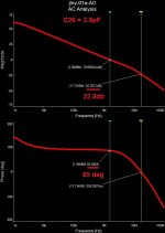
OK, here is what the stability margins look like in case I simulate your current schematic, but having C26=3.9pF (390pF simply "kills" both the phase and frequency responses - way too much). The global loop is good enough.
To have Gain = 28, make R46 = 27K
Now, if you leave the output stage as-is, it will most likely have local oscillation issues. So, the gate stoppers, the spreader, and lower quiescent current will help (as a minimum). The driver stage will improve the quality.
Attachments
This is back to your original circuit with just a few minor tweaks. It works in simulation, whether it works as well in practice remains to be seen... but I know nothing beats the thrill of getting sound from your first design
The bias preset should be 2.2k and you start with it set to minimum resistance. You turn the preset to increase the current drawn by the whole amp (which you will be monitoring) and you stop when it has increased by just 10 milliamps or so. Don't go any higher.
Notice the feedback resistor is 47k. This reduces the feedback factor and improves stability as Jan is suggesting.
(and don't forget the 10 ohm that goes in series with the 0.1uf cap on the output)
View attachment 529929
View attachment 529930
Yep - the OPS arrangement that may work
But still - be careful with the quiescent current, without thermo-coupled spreader (thermal feedback), runaway is always possible!
All,
I disassembled the power stage and rebuilt it according to Mooly's last post. However, for some reason, if the bias current reaches above about 100mA, the current instantly spikes up to well over 1A, tripping the current protection on my PSU. I have already tried putting two 0.56 Ohm resistors at the sources of the FETs, but this has made no difference.
For the record, I did start with the bias trimmer in the minimum resistance position, and turned it up EXTREMELY slowly. I have checked the system over to make sure I have assembled everything correctly and not shorted anything, but I have found nothing. Anyone have any thoughts as to where I may have gone wrong?
Last edited:
All,
I disassembled the power stage and rebuilt it according to Mooly's last post. However, for some reason, if the bias current reaches above about 100mA, the current instantly spikes up to well over 1A, tripping the current protection on my PSU. I have already tried putting two 0.56 Ohm resistors at the sources of the FETs, but this has made no difference.
For the record, I did start with the bias trimmer in the minimum resistance position, and turned it up EXTREMELY slowly. I have checked the system over to make sure I have assembled everything correctly and not shorted anything, but I have found nothing. Anyone have any thoughts as to where I may have gone wrong?
It may start oscillating at some tens MHz frequency, leading to current shoot-through rail to rail. All transistors close slower, then they open, so over certain frequency, one shoulder starts opening earlier, then the other one managed to close. The process is very fast, so in some cases you would not even see the oscillation itself - you just see immediate current increase.
By the way, I would set the quiescent current to around 120-150mA per pair for this topology - sort of a practical optimum for class AB regime with Laterals (as soon as you tame the oscillation).
However, for some reason, if the bias current reaches above about 100mA, the current instantly spikes up to well over 1A, tripping the current protection on my PSU. I have already tried putting two 0.56 Ohm resistors at the sources of the FETs, but this has made no difference.
The bias suddenly jumping up is a classic case of the circuit bursting into oscillation.
Have you added any supply decoupling to the output board ? You could try a small cap (say 10 to 100uf) directly across the two drains of the FET's.
Also in my last diagram I deliberately didn't add a small cap across the now 47k feedback resistor. You could try something really small like 10pf.
Although you can try turning the bias up to what happens, you mustn't run it at more than a few milliamps in this basic form because of the thermal runaway problems.
My system already has several thousand microfarads of decoupling caps in the vicinity of the power stage, as well as additional ceramic caps for RF decoupling. My scope is rated to 100MHz, so I will check again to see if that is what is happening. I will try adding a small capacitor across the feedback resistor. I may also try running the two boards from separate supplies again to see if that helps.
One important change to note is that in order to test the changes, I removed Q9 (Q7 on Mooly's schematic) from the low-power board and have migrated that and the power stage back over to a breadboard for testing. Effectively any changes to the power stage and biasing structure are fair game now, so we might look into other changes that may increase stability.
At some point, if we are unable to find a workable solution or I find that I have damaged the power transistors, I may call the experiment and redesign this amp from the ground up using the proper simulation techniques and thermal compensation that I have been shown here.
Once again, I will not be able to test the changes on the hardware until much later today.
All,
Success! On a hunch, I tried changing C19 to 10uF down from the massive overkill 470uF, and upon powering it back on, revealed my suspicion that the issue was, in fact, extremely low frequency motorboating rather than high frequency oscillation. The value of C19 was so large that the entire system was clamping down for several seconds at a time, and I, too skittish while adjusting the bias current, had been immediately turning it down before even one cycle could complete. Adding a few more 1000uF decoupling caps solved the issue in short order.
It seems the issue arose from the cheapo alligator leads on my PSU, which I measured to be adding about 2 Ohms of resistance in series with my power supply. plugging in a 2 ohm resistor in series with the power source in my simulation confirms this. When I finalize this design, I will likely have much shorter power leads, so this will likely be a fairly low risk, but I will still add in a few more capacitors than I think I will need just to be sure.
The last remaining issue that bothers me is the thermal runaway. Even using the revised biasing structure, the bias current continues to slowly creep up over time when not under active cooling. Would, perhaps, connecting a diode or two in series with the "bias-preset" resistor and tacking them to the heatsinks of the FETs possibly help this issue?
Attachments
All,
Success! On a hunch, I tried changing C19 to 10uF down from the massive overkill 470uF, and upon powering it back on, revealed my suspicion that the issue was, in fact, extremely low frequency motorboating rather than high frequency oscillation.
Hmmm
I'm saying nothing There is a lot going on, not just with the basic design of your amp but also its layout and implementation.What bias scheme are you using now ? If it uses a transistor as a 'vbe multiplier' then that transistor needs to be in thermal contact with the heatsink (one of them anyway).
- Status
- This old topic is closed. If you want to reopen this topic, contact a moderator using the "Report Post" button.
- Home
- Amplifiers
- Solid State
- AB amplifier is oscillating. seeking critique