Good day everyone
I am currently working on a stereo 3-Way active crossover system. This means that I will need six power amplifiers.
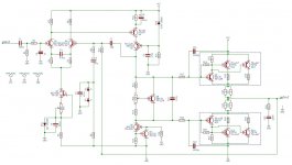
I have taken a design published in ETI October 1993 for a 50W 8 Ohm amplifier and slightly changed the design. I have a few questions with regards to the design (see attached schematic).
1. The article calls for MKM capacitors, may I use any film type capacitors for those?
2. Some of the capacitors are shown as electrolytic in the schematic, but the BOM calls for ceramic capacitors, like C5 & C6.
3. The schematic calls for 220uF capacitors for C3 & C8, but the BOM calls for 2200uF. Which will be the correct value.
4. Q3 calls for BF245A, which seems to be obsolete, what would be a good replacement part?
5. The original design used BDT64/BDT65 darlington units for output transistors. I replaced them with a compound arrangement (in the blue border) using the (almost) same resistor values as in the BDT64/65 datasheet. Will this work or am I missing something? Would it be better to only use TIP142/TIP147's? Rod Elliot is convinced that the compound arrangement causes lower distortion than the darlington arrangement. NAD also uses the compound arrangement in their designs.
I used two output transistors in parallel, this will sort out any possible dissipation problems with the high current required for a 4 Ohm load.
Any advice and inputs will be appreciated!
I am currently working on a stereo 3-Way active crossover system. This means that I will need six power amplifiers.
I have taken a design published in ETI October 1993 for a 50W 8 Ohm amplifier and slightly changed the design. I have a few questions with regards to the design (see attached schematic).
1. The article calls for MKM capacitors, may I use any film type capacitors for those?
2. Some of the capacitors are shown as electrolytic in the schematic, but the BOM calls for ceramic capacitors, like C5 & C6.
3. The schematic calls for 220uF capacitors for C3 & C8, but the BOM calls for 2200uF. Which will be the correct value.
4. Q3 calls for BF245A, which seems to be obsolete, what would be a good replacement part?
5. The original design used BDT64/BDT65 darlington units for output transistors. I replaced them with a compound arrangement (in the blue border) using the (almost) same resistor values as in the BDT64/65 datasheet. Will this work or am I missing something? Would it be better to only use TIP142/TIP147's? Rod Elliot is convinced that the compound arrangement causes lower distortion than the darlington arrangement. NAD also uses the compound arrangement in their designs.
I used two output transistors in parallel, this will sort out any possible dissipation problems with the high current required for a 4 Ohm load.
Any advice and inputs will be appreciated!
Attachments
Last edited:
I don't know what MKM capacitor is.
Electrolytic are generally used where high values of capacitance are required.
Ceramic capacitors are used where very low inductance and lowish esr are required. They do quite different jobs and are not usually swapped.
C3 could be any value from 1uF to 220uF
C8 is an AC bypass, I don't know what the Designer intended, if there is a contradiction in the build notes.
BF245a is used as a CCS for the LTP tail.
Any CCS will work here.
Any jFET configured as a CCS will work here.
You have swapped from an integrated Darlington to a discrete CFP (Compound Follower Pair).
The CFP is reputedly very difficult to stabilise and great "designer" skill is needed to compensate the final solution.
Change it to a normal discrete double EF.
Start with a 1pair output stage and get it working properly. Then increase to a two pair and retest and check the compensation/s.
BTW, 50W into 4ohms usually needs a 1pair output stage, 1pair of 130W devices has a reliable maximum output power of ~50W
Or start with a design that has been recommended here AND has a comprehensive BUILD GUIDE that is known to be good !
Last edited:
Thanks Andrew!
I've noticed on several discussions that oscillation may be a problem with the CFP. I will build one board with a single pair and test it first. If I struggle too much I will just revert to the original design using TIP142/TIP147's for the complete project (Stereo 3-way active crossover).
The original design is for 50W into 8 Ohms. I intend to use it to deliver 100W into 4 Ohms. Furthermore I have a hunch, and it is really just a hunch, that transistors may generate less distortion if they are not working too hard (if there is evidence/experience to the contrary please correct me) . So I would like to try the parallel output transistors.
If so, rather go with a Darlington made up of two discrete transistors (EF2). General purpose Darlington transistors are not well-suited to audio power amps, they have like 2 kOhm emitter resistors for the drivers when you'd rather want around 220 ohms (or even 100-120 ohms in some cases), giving very low driver current and slow base charge depletion in the outputs. This negatively affects gm linearity (which you should be concerned about with 4 ohm loads) and shoot-through at high frequencies.If I struggle too much I will just revert to the original design using TIP142/TIP147's for the complete project (Stereo 3-way active crossover).
CFP outputs can't be that hard to stabilize either, Rod Elliott's P3A uses one. He notes that the lower leg (pnp driver, npn output) can often use a small capacitor across driver B-C though. The main problem with CFPs is that the outputs can be driven into saturation and then take quite some time to recover, which is not exactly doing clipping behavior any favors. Speaking of which, study what the VAS is doing as well.
EF2 is kinda starting to be pushing it for a 100W/4R spec. Good, fast modern transistors with low beta droop are advised. Back in the day they would have gone with an EF3 instead (e.g. Leach amp), but those are a fair bit harder to make work. Two pairs of outputs is definitely a good idea already.
The bias arrangement shown here is straight '70s Elektor, it is not inherently safe in case of bad contact in the pot. Use one with the adjustment pot in the B-E leg instead.
The cascode VAS may not be such a good choice here, Samuel Groner notes fairly high sensitivity to nonlinear loading by the output stage (and with 4 ohms on an EF2 you are likely to see that). A buffered job may be a better idea. Or buffered cascode maybe, though circuits with 3 transistors tend to be harder to stabilize. (With no cascode you're at the mercy of VAS transistor quality again, specifically low Cob.)
Last edited:
Thank you for all the comments!
I've bought all my components for two channels and JHL's PSU over the weekend. I will have to redesign the constant current source as the BF245A is discontinued and no direct replacement available.
Then I will continue to the layout, if all goes well I will be able to post the layout soon")
I've bought all my components for two channels and JHL's PSU over the weekend. I will have to redesign the constant current source as the BF245A is discontinued and no direct replacement available.
Then I will continue to the layout, if all goes well I will be able to post the layout soon
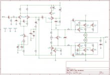
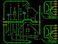
I've eventually got round to do the PCB layout. Here is the schematic and PCB, I used the layout as published in ETI for the input and VAS, but had to make my own plan for the output stage.
I am not well versed in the pitfalls related to PCB layouts, please inform me if anything in my layout may result in unwanted effects...
I am not well versed in the pitfalls related to PCB layouts, please inform me if anything in my layout may result in unwanted effects...
Attachments
- Status
- This old topic is closed. If you want to reopen this topic, contact a moderator using the "Report Post" button.
- Home
- Amplifiers
- Solid State
- 100W 4Ohm load Amplifier Design