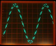
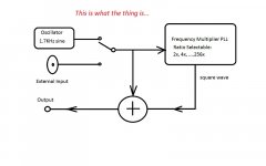
Sometimes we would want to see a power amp's response to a stepped signal when it is driven approaching the rails, because that could be where the amps weak spots locate that rarely show up at "normal" operation levels and signals, yet we would not quite want to drive the amp with a full amplitude square wave to smoke or stress the Zobel networks. A jagged sine wave then becomes useful.
This is a generator I designed and built recently for that particular signal and purpose, I call it Bubba-Jag. It has a Bubba oscillator that generates a 1.7 KHz Sine wave, and a PLL that phase-locks onto that sine wave and generates square wave of frequency at multiple that of the sine wave (the pictures show 16x). These two then combine together to become a jagged sine wave.
The phase locking is important here as otherwise a stable, non-moving image when probed with a scope is not possible.
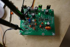
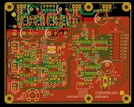
The assembly is on a 100x80 mm^2 double sided PCB, SMD parts are used but they are all hand-soldering friendly. It could make a SMD starter's project as well for those who have never done SMD before.
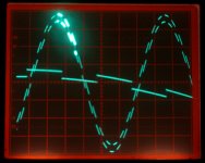
This is a generator I designed and built recently for that particular signal and purpose, I call it Bubba-Jag. It has a Bubba oscillator that generates a 1.7 KHz Sine wave, and a PLL that phase-locks onto that sine wave and generates square wave of frequency at multiple that of the sine wave (the pictures show 16x). These two then combine together to become a jagged sine wave.
The phase locking is important here as otherwise a stable, non-moving image when probed with a scope is not possible.
The assembly is on a 100x80 mm^2 double sided PCB, SMD parts are used but they are all hand-soldering friendly. It could make a SMD starter's project as well for those who have never done SMD before.
Attachments
Congratulations on a very nice-looking result! Bravo and well done.
Here are a couple of comments about the schematic.
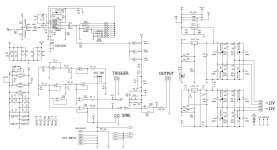
If you're concerned enough to install eight copies of a (2C+1R) snubber, one copy per diode on each of your bridge rectifiers (D2-D9), then why not also choose excellent diodes with much less turnoff snap than the 1N4001? This diode is in the same package as the 1N4001 but performs FAR better, at least in these tests. Belt and suspenders and elastic waistband too.
It's surprising to see (digital gate) --> (series resistor) --> (digital gate) on a small PCB using 74HC logic. The 74HC risetime has got to be much much longer than the propagation delay down the longest transmission line on the board, so reflections are not much of an issue. Specifically R28, R10.
Here are a couple of comments about the schematic.
If you're concerned enough to install eight copies of a (2C+1R) snubber, one copy per diode on each of your bridge rectifiers (D2-D9), then why not also choose excellent diodes with much less turnoff snap than the 1N4001? This diode is in the same package as the 1N4001 but performs FAR better, at least in these tests. Belt and suspenders and elastic waistband too.
It's surprising to see (digital gate) --> (series resistor) --> (digital gate) on a small PCB using 74HC logic. The 74HC risetime has got to be much much longer than the propagation delay down the longest transmission line on the board, so reflections are not much of an issue. Specifically R28, R10.
Congratulations on a very nice-looking result! Bravo and well done.
Here are a couple of comments about the schematic.
If you're concerned enough to install eight copies of a (2C+1R) snubber, one copy per diode on each of your bridge rectifiers (D2-D9), then why not also choose excellent diodes with much less turnoff snap than the 1N4001? This diode is in the same package as the 1N4001 but performs FAR better, at least in these tests. Belt and suspenders and elastic waistband too.
It's surprising to see (digital gate) --> (series resistor) --> (digital gate) on a small PCB using 74HC logic. The 74HC risetime has got to be much much longer than the propagation delay down the longest transmission line on the board, so reflections are not much of an issue. Specifically R28, R10.
Thank you Mark!
I agree with you that most all parts you mentioned in your comments are redundant. For the rectifying diodes I have "beep"-load of 1n4004 and I want to use them up (and I may not be alone in the forum). The diode switching noise is not a concern in this application but I copy-paste the layout of power supply including regulators from my other project, decided to leave the snubbers in just in case. Your recommended low noise diode is good info that I have never paid much attention to, much appreciated.
I also agree with you that the transmission line effect is not a concern on this PCB at all. However I took a design habit of always isolating a load from the driver's power/GND rails, hence the redundant resistors resembling source terminating resistors. In the schematic all six gates in the hex inverter U8 are used and they likely switch at a same moment, I thought it would be some sort of safe guard to put an output resistor where it could matter, as long as it is not damaging. Bottom line: from a PCB designer's point of view these could all be jumpered out if found unnecessary, and better to have them there than nothing to resort to in case things come up. --I am perhaps a pessimist when it comes to PCB design
")
... connect an external function generator to this
If you propose to apply external inputs from 20 Hz to 20 kHz, that would require the PLL to have an exceptionally wide capture range. I doubt the CD4046 could do it without range-switching or other divide and conquer techniques. It would require a somewhat dramatic increase in complexity.
If you propose to apply external inputs from 20 Hz to 20 kHz, that would require the PLL to have an exceptionally wide capture range. I doubt the CD4046 could do it without range-switching or other divide and conquer techniques. It would require a somewhat dramatic increase in complexity.
Yes, there might be increased circuit complexity. Low frequency is not so much of interest, but at 20kHz investigation and tweaking could be very useful and interesting using this Bubba-Jag.
If a number of weeks go by and nobody has provided to you a modified circuit design, I suppose you could make your own changes to the original "no other frequency except 1.7 kHz" design, centered at 20 kHz: I suppose you could make a second PCB with a second set of parts+values which creates a "no other frequency except 20.0 kHz" design. Maybe this is all you would ever need. Or maybe you might decide that you need this 20 kHz board, AND the original 1.7 kHz board, AND also a third yet-to-be-disclosed board that gives "no other frequency except 130 Hz" capability. Maybe three single-frequency boards, give higher performance than one multi-frequency board (?). Certainly the PLLs would be a lot more selective on the single-frequency boards.... at 20kHz investigation and tweaking could be very useful and interesting using this Bubba-Jag.
If a number of weeks go by and nobody has provided to you a modified circuit design, I suppose you could make your own changes to the original "no other frequency except 1.7 kHz" design, centered at 20 kHz: I suppose you could make a second PCB with a second set of parts+values which creates a "no other frequency except 20.0 kHz" design. Maybe this is all you would ever need. Or maybe you might decide that you need this 20 kHz board, AND the original 1.7 kHz board, AND also a third yet-to-be-disclosed board that gives "no other frequency except 130 Hz" capability. Maybe three single-frequency boards, give higher performance than one multi-frequency board (?). Certainly the PLLs would be a lot more selective on the single-frequency boards.
Yes, you are right, I could, maybe I should look into that.
Happy Holidays
It's not hard to switch between an external signal and the Bubba oscillator. For example we can ground C3 and inject an external signal at C6. The VCO of the 74HC4046, operating at 5V, has a tuning range of slightly less than three octaves for a given set of timing components and will track the external signal within that range. By making the VCO timing resistor a pot we can slide that three-octave range over a broad band of frequency.
Bubba-Jag can now take external input
I made changes to the design.
With a shorting jumper and a trim pot, we can now switch between the on-board Bubba sine oscillator and an external input fed through a BNC connector. The trim pot adjusts the center frequency of the PLL's capture range allowing it to lock onto the incoming signal at frequency of choice. According to 74HC4046 datasheet, the VCO of our circuit will be able to operate up to over 600 KHz, or lock onto up to 20KHz external input at 32x multiplication. It can go even higher by using a smaller value capacitor C9.
Attachments
Anyone wants PCB?
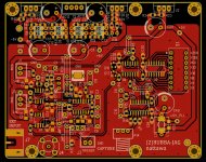
Is there interest out there in the revision-2 Bubba-Jag PCBs? (layout and schematic attached) I'll soon be able to order a batch of 10 at a very good price, and wondering if I should order more than one batch just in case there is demand, despite the SMD based design. The cost per PCB should be about us$2 or so if there would be no surprises.
Is there interest out there in the revision-2 Bubba-Jag PCBs? (layout and schematic attached) I'll soon be able to order a batch of 10 at a very good price, and wondering if I should order more than one batch just in case there is demand, despite the SMD based design. The cost per PCB should be about us$2 or so if there would be no surprises.
Attachments
- Status
- This old topic is closed. If you want to reopen this topic, contact a moderator using the "Report Post" button.
- Home
- Amplifiers
- Solid State
- Bubba-Jag