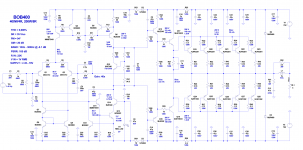
I agree.....................The OPs's circuit could be improved if the current source facing the TIS/VAS had its own control transistor. .................
C4 seems a bit small.
It rolls off the amplifier before the input filter.
I suggest you increase it to meet this condition
C14> sqrt(2)*C1*(R1+R2)/R10 >4u7*(1k+27k)/0k68 > 193uF, use 220uF, or 330uF
Add in D.Self/Hawksford Vbe multiplier resistor. It corrects the output voltage to be more constant for small changes in VAS/TIS current up through to the source/sink.
You need to turn around the Vbe multiplier so that the resistor ladder comes under the VAS/TIS and the transistor follows. Then add in the resistor (10r to 22r depending of current) between the ladder and the transistor collector.
I like the flexibility of base stoppers for all three output stages and the 100pF of Cbc. Easy to place, or omit.
400W into 8r0 from +-90Vdc supplies is possible, if you build for adequate current capability.
But I doubt tht 800W into 4r0 is possible the voltage droop in the supply rails will probably be too high. May need nearer +-95Vdc to hit that target.
You have lot's of MF local decoupling. Look at leaving spaces/pads for HF local decoupling, especially around the driver and pre-driver.
You have no HF decoupling in the front end !
Do make sure you have a Power Ground that feeds along side adjacent supply rails, or even better under adjacent supply rails (low loop area = low impedance = low interference).
Last edited:
The 230W MJL4302/4281 are marginally faster and just about match the fastest Sankens.If I recall correctly, the reason they were failing was because slow output devices don't shut off fast enough and can suffer from shoot through. Ostripper was recommending 30mHZ minimum.
I used Sanken 2SA1295/2SC3264. Ostripper and I both found these run cooler. Your NLW1302/3281 were popular for his designs too.
exceeding 50MHz in parts.
The 230W MJL4302/4281 are marginally faster and just about match the fastest Sankens.
exceeding 50MHz in parts.
Yes these are another good choice. They weren't available for a while in North America, but seem to have reappeared.
Thank you AbdrewT for your useful comments.
Sorry for the misunderstanding. I omitted the HF decoupling on the schematics but in reality I intend to put 100nF MLCC cap on every electrolytic cap.
I do not understand. You said first that C4 is a bit small and then suggest to increase C14. Is that an error ? Are you reffering to increase C4 ?
Sorry for the misunderstanding. I omitted the HF decoupling on the schematics but in reality I intend to put 100nF MLCC cap on every electrolytic cap.
I do not understand. You said first that C4 is a bit small and then suggest to increase C14. Is that an error ? Are you reffering to increase C4 ?
Last edited:
H.Ott was specifically talking about smd capacitors for HF decoupling in very fast circuits.
He said something along these lines.
Find the smallest package that can be placed close enough to minimise the impedance of the current route.
Then select the highest capacitance available in that package.
Applying that rule to through hole capacitors and one would use 220nF (50V, or 100V) in the 0.1" or 0.2" ceramic with the shortest possible through hole leads.
No.////////////// I omitted the HF decoupling on the schematics but in reality I intend to put 100nF MLCC cap on every electrolytic cap.
Put them right beside the lead out of the device demanding the changing current,
i.e. right next to the collector of the pre-driver of the triple EF.
The electrolytic because it is 10000 times bigger, ends up too far away from the device lead out.
AND, when one places a low esr capacitor on an electrolytic with inductance between them and almost no resistance to damp, one can end up with more ringing, rather than less ringing.
One needs resistance between the capacitors to damp the ringing when current changes.
The OPs's circuit could be improved if the current source facing the TIS/VAS had its own control transistor. The thrift that saves 25-cents on the BJT and extra Rs and Cs also sacrifices speed in this stage.
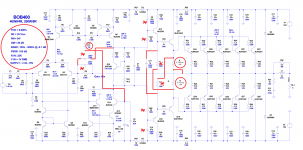
Do you mean like this ?
An externally hosted image should be here but it was not working when we last tested it.
Hi Guys
In post-19 the OP said that there was cross-over distortion with the 21194/93 but not with the 1302/3281. I would ask if the idle current had been optimised for each device, or did you simply make a swap and run the circuit without checking current?
The point is that there is crossover distortion with all devices at low to moderate bias, and this can be eliminated if the bias is extremely high (class-A).
The data displayed in the lower left corner of LTspice usually has prefixes that are easy to miss. For example, you might hover the cursor over an output BJT and expect it to idle at 8W. If the bias regulator has not been adjusted, maybe you see an "8" and a "W" but there might be a tiny 'f' in between for femto - no heat at all.
Yes, the figure in post-28 is what I referred to. This enhances speed of the TIS-VAS. A 15pF cap from the base of Q8 to the collector of Q9 also helps increase speed and reduce high-frequency THD.
Slew rates do not have to be symmetric as long as both numbers are greater than that required for the largest, fastest signal. Even with that detail satisfied, one still wonders if the asymmetry might impart something on the output or reflect other attributes less desireable for audio? Personally, I prefer symmetric circuits partly for this reason.
Have fun
Do you think it's ok with that speed up cap or I should change the output stage configuration for my 4MHz devices ?
You can reduce the slew rate.
Yes, the images in post #19 are showing the collector currents of the output devices, not the voltage at the output. Of course I've biased the output stage at 30mA. THD is 0,01% at 10KHz full power. And it will be much lower if I use KSC3503/KSA1381 in VAS and pre-drivers, but these are another hard to find devices with the same hfe class.
You can reduce the slew rate.
How do you do that?
yes.Do you mean like this ?
An externally hosted image should be here but it was not working when we last tested it.
I see base stoppers on Q3 & Q8.
Q.) Do we need base stoppers on Q4 & Q9?
How do you do that?
Many ways. Example: reduce tail current of LTP, change the compensation.
")
yes.
I see base stoppers on Q3 & Q8.
Q.) Do we need base stoppers on Q4 & Q9?
Needed on Q9, unless you like your amp locking to the positive rail on clipping.
Not really needed on Q3 and Q8.
- Status
- This old topic is closed. If you want to reopen this topic, contact a moderator using the "Report Post" button.
- Home
- Amplifiers
- Solid State
- 800W Power Amplifier