Tube_Dude said:
Because the down side of R2 is keped fixed a one diode drop from the + rail...you forget the emitter resistor...")
you can add the emitter resistor there. Because of the CCS (I2) for Q3, the emitter resistor is nothing more than an increment to the Vbe of Q3.
it does not change the nature of this discussion: LTP by itself cannot split current evenly between two arms. That is the central assumption in your calculation of Iq for VAS.
Olá Eva
Can you please explain to me that result??
Saludos!!
Can you please explain to me that result??
And with 1.38mA, the VAS is biased at : (1.38-1)*14.47 = 5.5 mA
Saludos!!
Eva said:So in the end, assuming ideal identycal transistors and resistors we must have 2.76/2 = 1.38mA in each leg of each LTP
you basically assume the conclusion here,
.We know enough about the currents in Q3!
The collector current is about 2mA + some µA.
So the current into the basis of Q3 may be 10µA,
in any normal case small compared to the current through R2,
so the current through R2 is dominantly defining the collector
current of this tail of the differential amp.
The collector current is about 2mA + some µA.
So the current into the basis of Q3 may be 10µA,
in any normal case small compared to the current through R2,
so the current through R2 is dominantly defining the collector
current of this tail of the differential amp.
ChocoHolic said:so the current through R2 is dominantly defining the collector
current of this tail of the differential amp.
the current through R2 is determined by the Vbe drop of Q3 and R2's value,
it is not for a reason that the voltage drop off R2 is precisely 0.65v no matter what the value of R2 is (within a range, again).
millwood :
The schematic you've posted is the classic prototype of LTP mismatching, no doubt
But adding small emiter degradation resistors to the LTP and trimming R2 for equal voltage drop on them solves the problem
You still have the imbalance caused by Vbe variations in Q3 with temperature but this could be cured by degenerating Q3 adding an emitter resistor and fixing its gain
This temperature dependent imbalance is much less apreciable in the complimentary LTP+VAS topology since both VAS suffer similar Vbe variations
Bias current will increase with temperature. Heating junctions by 75ºC could mean 150mV [2mV/ºC] reduction in Vbe and 150mV/47 = 3.19mA of bias increase, totalling 8.7mA and thus further heating and further bias increase, maybe even thermlal runaway [another reason to paralell two or three 2N5401/5551 on each side]
Yes ...that's rigth...because of that and because Vbe is a parameter that change a lot with temp. we need the emiter resistor...millwood said:
the current through R2 is determined by the Vbe drop of Q3 and R2's value,
Eva said:millwood :
The schematic you've posted is the classic prototype of LTP mismatching, no doubt
But adding small emiter degradation resistors to the LTP and trimming R2 for equal voltage drop on them solves the problem
1st of all, emitter resistors on the input resistors will reduce mismatch. However, we are talking about perfectly matched transistors here. adding emitter resistors does not help.
2ndly, if you have to trim r2 to equalize the current, what does it say about the statement that "LTP current is evenly split between the two legs"?
all this simulation does is to show that no matter how matched the transistors are, you will NOT get evenly split current in LTP automatically.
Once you have that assumption taken out of Tube_dude's calculation, you will not be able to calculate the current in the original schematic.
temperature doesn't play a role in this discussion so we should keep it out of this discussion all together.
Tube_Dude said:
Yes ...that's rigth...because of that and because Vbe is a parameter that change a lot with temp. we need the emiter resistor...
good, we are making progress.
Once you agree with that, your job becomes "easier": how do you find out the voltage drop on the emitter resistor (R15?) on the original schematic? Don't go back to assume the voltage drop on that 680ohm resistor first - otherwise you are going in circles.
Tube dude :
Try to simulate a complimentary LTP with complimentary VAS like the one we are talking about
Then you may end understanding that both LTPs mutually balance themselves through the VASs
In your cirtcuit you don't have any lower LTP nor VAS to balance the upper ones, just 2mA fixed current sources. Also, the VAS has a huge gain [no degradation] so adding a lower LTP and VAS will result in a huge biasing in the VAS [about 30mA assuming Vbe=700mV and beta=100 for 2N5401/2N5551]
Please try it...
Edit : In the complimentary version the remaining 349uA will be forced to flow into Q3 base [producing 30-60mA VAS biasing or more]
Hi Millwood!
Again.
In your circuit and without emitter resistor, yes.
But now simulate it with 100 Ohms in series to the emitter of Q3
and 33 Ohms in series of each emitter of Q1 and Q2...
==> better current balance.
....and now double it complementary...
You should find good current balancing then.
(hope your simulation does not start to oscilate, probably not...)....
Cheers
Markus
millwood said:
good, we are making progress.
Once you agree with that, your job becomes "easier": how do you find out the voltage drop on the emitter resistor (R15?) on the original schematic? Don't go back to assume the voltage drop on that 680ohm resistor first - otherwise you are going in circles.
Current in the LTP tail (assuming the 2,8 volts LED voltage you pick)---2,8 -0,6=2.2
2.2 V /470 = 4,6mA
2,3 mA in each arm of the LTP.
Voltage drop in the colector resistor of the LTP 680X 2,3mA=1,56
Current in the VAS...1.56-0,6=0,96V
0,96/47 Ohm=20mA
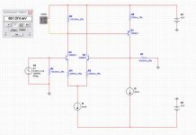
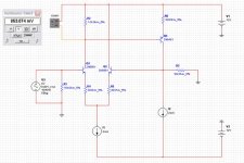
For the single ended example try R2 = 1k and R6 = 175
For complimentary LTP I've explained already the criteria :
- Both VAS have the same gain and the same turn-on point
- The balance in the VAS [0A amplifier output current] is reached when both input currents into the VAS are the same [thus both LTPs having the same output]
- Since outputs from the LTPs are fully complimentary [one increases when the other decreases, the point where they are equal is the exactly the balance point of the LTP [equal currents on each leg]
ChocoHolic said:Hi Millwood!
Again.
In your circuit and without emitter resistor, yes.
But now simulate it with 100 Ohms in series to the emitter of Q3
and 33 Ohms in series of each emitter of Q1 and Q2...
==> better current balance.
Cheers
Markus
"better" or not depends on where your starting point is. In this case, the starting point is that the Ir2 is less than half of the tail current. so increasing the voltage drop on R2 will move it towards the 1ma point.
but if we had used a smaller R2, we would have been worse off with the use of that emitter resistor on Q3.
Again, as long as you don't assume that the LTP by itself will split the current evenly, you cannot calculate the current (for the leg and for VAS) in the original schematic.
The sole purpose of this simulation is to show that, with numbers, so people will have easier time to understand the "key" drivers here. Emitter resistors certainly aren't one of those key drivers.
Tube_Dude said:2.2 V /470 = 4,6mA
2,3 mA in each arm of the LTP.
Dude, you are going in circles,
.That's the single biggest flaw in this discussion, and the simulation was to show you that an ltp will not by itself automatcially balance leg current.
AAAAAAAAAAAAAAAAAAAAAAAAAAAAAAAAAAAAAAAAAAAAAAAAAAAAAAAAAAAAAAAAAAAAAAAAAAAAAAAAAAAAAAAAAAAAAAAAAAAAAAAAAAAAAAAAAAAAAAAAAAAAAAAAAAAAAAAAAAAAAAAAAAAAAAAAAAAAAAAAAAAAAAAAAAAAAAAAAAAAAAAAAAAAAAAAAAAAAAAAAAAAAAAAAAAAAAAAAAAAAAAAAAAAAAAAAAAAAAAAAAAAAAAAAAAAAAAAAAAAAAAAAAAAAAAAAAAAAAAAAAAAAAAAAAAAAarg,
Eva said:For the single ended example try R2 = 1k and R6 = 175
the reason you choose R6 that way is you know the Iq for the VAS. in the origingal schema, you don't.
that's the whole point sreten and I have been saying.
- Status
- This old topic is closed. If you want to reopen this topic, contact a moderator using the "Report Post" button.
- Home
- Amplifiers
- Solid State
- 150W Is it good?