Hi there!
Need some help with this circuit (attached)...
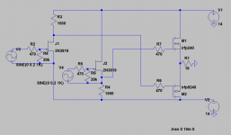
There is a balanced input, then two jfets pre-amplifying and biasing the output mosfets (it's direct coupled). The problem is at the balanced input; the hot and cold enter to the jfet gates, BUT i cannot short the references (the jfet sources). Two separate signals works, but the standard balanced have a common (pin 1 in xlr) so it would short [R4].
Is there any way to solve this without transformers? maybe something like a virtual ground..? Preferably a direct coupled workaround.
In the circlotron article (https://www.passdiy.com/gallery/amplifiers/build-the-amazing-fet-circlotron) there's a virtual ground. Maybe this helps...
Thanks!!!
Note: The mosfets, biasing and others are only representative, i don't have the spice models for the parts i'll use.
Need some help with this circuit (attached)...
There is a balanced input, then two jfets pre-amplifying and biasing the output mosfets (it's direct coupled). The problem is at the balanced input; the hot and cold enter to the jfet gates, BUT i cannot short the references (the jfet sources). Two separate signals works, but the standard balanced have a common (pin 1 in xlr) so it would short [R4].
Is there any way to solve this without transformers? maybe something like a virtual ground..? Preferably a direct coupled workaround.
In the circlotron article (https://www.passdiy.com/gallery/amplifiers/build-the-amazing-fet-circlotron) there's a virtual ground. Maybe this helps...
Thanks!!!
Note: The mosfets, biasing and others are only representative, i don't have the spice models for the parts i'll use.
Attachments
Have you thought what will happen if J1 is off and J2 is on? M1 and M2 bang!
mmm... you say in the case that J1 fails? M2 just keep unbiased and M1 stays safe...
This circuit is wrong on so many levels it's not even worth commenting. Even so, here's a hint:
How are your JFETs biassed? What kind of signal does the output satge need, single ended or balanced? How is bias current fot ghe output stage set and tracks temperature?
ok....
consider that the circuit is just representative... the actual parts will be different but the concept is the same.
The input stage will use depletion mode mosfet, they are self biased and happy at zero volts, so they only need a resistor from gate to source to bias them. The output stage will need single ended signal, the input will be balanced. The input stage do that, the balanced signal enter and outs two single ended signals with some voltage offset that will bias each output mosfets at 4.4[V] aprox between its gate and source. The output mosfets will be lateral parts so there's no need for temperature compensation.
PLEASE get yourself a book with some electronics theory and have a read. Poking around in a simulator will NOT help you understand a circuit if you throw it around with nothing but wishfull thinking to guide you - like looking just at one aspect of a circuit you like and disregarding all the consequences that come with it. In some cases these will make the circuit impractical or even impossible to realize in the real world.
First, what is it you are trying to do, does your circuit need to have gain or not?
Second, when you pose a question, you do NOT explain which devices you are going to use halfway in the thread, having specifies something completely different in the attached schematics. It annoys people to waste time analyzing a circuit which you are actually NOT making.
Third, know your devices and how they work:
- do you know that even assuming your input stage can swing all the way to the supply rails without any loss (which it can't) your output stage with an 16 ohm load will at most output about 12V peak, so 2V out of your 14V rails will be wasted on the MOSFETs. The situation gets drastically worse as the load is reduced - also a lot of nonlinearity will be added due to the inherent asymetry of the P and N MOSFET, which includes DC offset.
- are you sure zero bias is the most linear operating point of your input stage? Drawing JFETs here is EXTREMELY misleading.
- Real components have tolerances. Your 'constant DC difference between the gates of the output MOSFETs' may be constant once the circuit works, but it has to be adjustable, so the circuit has to provide for it from the get-go. Input FETs have tolerances (possibly quite large ones) so there must be a means to get around that - NOT specifying things like 1550 ohm resistors. You won't know the actual value until the circuit is built with a real part, and they will be different for the two, so there must be some sort of balance control toi prevent combinations that would be lethal for the circuit.
- Is your balanced input signal what exits your signal source, or do you have two actual signals which are equal in amplitude but reversed in phase? If so, are these isilated like in the schematic (transformer?) or is there a common pin or a known DC difference between them?
I have not even started analysis of your schematic.
First of all, for one input you are taking output from the drain of the FET, for another on the source. The first implies voltage gain (how much? See: component tolerances!), the second is a follower. Equal resistors will mean nothing except at DC so obviously the circuit does not satisfy the requirements of the output stage at the get-go. And it's not a question of 'help' - it's simply the wrong circuit to use for that output stage.
Secondly, when you state that you need a circuit that converts a differential input signal to two single ended signals with a constant DC offset, you are actually formally stating this needs to be a differential to single-ended converter - DC offset to be added for the second output as the basic circuit makes possible. There are a number of circuits that will do this - again,, you do not specify gain, so that makes it difficult to choose - and you can simply look them up and adapt. Instead, you have decided to use a 'new' approach. The hallmark of all classic diff to single ended converters are that the signal paths for each of the differential inputs are connected, which is what differential implies - output = G(V1-V2). You can't make a circuit like that without it, unless some assumptions are ALWAYS satisfied, such as input signals are always both present and always equal and opposite in phase. and in some cases, isolated (floating). However, even then the circuit may really need some sort of connection to cancel out component tolerances.
Thirdly, your output uses ground reference, i.e. the load ties to ground. However, there is no realy clear reference for the inputs - the upper MOSFET one floats, the lower MOSFET one has -14V reference. Are you sure there is NO (and I mean NONE whatsoever) hum and noise in the 14V line, compared to ground, which the input might amplify or at least relay to the output because it is not clearly referenced? Here is one more example of something that will work in a simulator but completely hides a real problem in the real world, which would require an eventual re-design of the circuit to work properly in said real world.
Fourthly, if you have two signals which are equal and opposite in phase, are you sure the complementary output stage is the best option? A quasi complementary would be the natural choice, and before you ask, YES it would be completely symmetrical in operation - in fact the only way to insure this is to use two floating signals opposite in phase.
So, what do we have as a result? You have decided to be fancy in your choice of components without really understanding all the ins and outs of their operation, and without understanding the circuit topologies. i.e. prior art that is used to accomplish what you want. As a result you are trying to marry three circuits that can't work together in this manner because you do not understand how they work (clue: connection of the inputs, common drain vs common source). This circuit needs far more help than the input stage, starting with euthanasia of the actual one drawn and going back to the basics. Or, you are asking everyone here to literally invent a new circuit using your favored components - and explain how it works and why it is the way it is. It has taken me over an hour to just write the above, and the proper treatise of how and why your circuit fails to do what you want it to do would require writing a small book. And THEN as this was being done, it would be shown how and why to do it - still using your favored components, which is a whole process of design and simulation.
I am sorry, I do not mean to insult, but you have shown painfully too little effort of your own to ask everyone here to invest the effort needed to solve your problem, which is why your thread has had so few answers. In fact, I would hazard to think some people who could say a lot more on this subject than I can did not contribute because they find such requests... well, insulting. Investing an hour an a half of your time into reading about circuits that are well known to do what you need would have given you a lot more insight, likely enough to design a circuit that works - yet I have now invested this much and more time just to show you where to look at for problems in your circuit, with no solution, in the hopes you will apreciate what I am trying to do, and understand where the real problem is - and it's not the input stage - because this is the extent I am willing to go to, and no further.
Last edited:
I got books. And it seems you don't understand some topologies, like cathode loading (in this case source loading) with full gain. IT'S NOT A FOLLOWER. If you want to understand that topology, read chapter 12 section 6 of RCA Radiotron Designer's Handbook.
I didn't query for help for the entire circuit; the other parts are my problems.
Please don't make asumptions without knowing...
Also you should read the biasing info in the same book, you'd be surprised the networks it shows.
You also didn't understand my first post, it says "i don't have the spice models for the parts i'll use." That's why i don't post the actual circuit, so stop complaining about a circuit that will not exist; the one i post is just a example, as i said before.
If you hate 'new' approachs that's your problem.
It's perfectly posible not to reference the signal to ground, and without noise issues. Again, chapter 1 section 3.
The quasi-complementary circuit is great, but it gives current and voltage gain not in a so linear way, at least with the mosfet parts the market offers; i do prefer current 'gain' for the linearity subject. If you hate complementary circuits... maybe you also hate pass designs. I did a (real, not only simulated) circuit with two n mosfet parts, but with another topology and it sounds excelent. And it's not a conventional circuit.
You are wrong when you say i don't understand connection of the inputs, common drain vs common source; in fact you probably don't understand different input and biasing networks (now refer to the biasing info in the first chapter).
Your are probably stuck with the same conventional topologies all commercial amplifiers have; feel sorry for you.
Finally, i did say i'll not use jfets.Tthe parts i'll use works most linear at zero volt bias.
I leave.
Bye.
- Status
- This old topic is closed. If you want to reopen this topic, contact a moderator using the "Report Post" button.
- Home
- Amplifiers
- Solid State
- Input stage help needed