I am trying to build a preamp with tone controls, based on the circuits in Randy Slone's "Audiophile Projects Sourcebook." I've combined the circuit for his basic gain stage + loudness + volume control, with his circuit for a three-band tone control, and inserted a switch for bypassing the tone controls.
Even though the essential design is in most respects a straight copy from his book, I have many questions about the actual implementation. And those are the questions I'll list below, but first I thought I'd include the schematic and give some explanatory notes.
Tarun
Even though the essential design is in most respects a straight copy from his book, I have many questions about the actual implementation. And those are the questions I'll list below, but first I thought I'd include the schematic and give some explanatory notes.
Tarun
Attachments
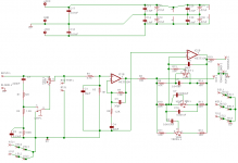
Some explanations about circuit
A lot of the explanations may be unnecessary if you have read Randy Slone's book from which I've got the schematic. Those of you who are beginners to audio amps like me, and who want to build a good preamp, may like his book. I know I learned a great deal from it.
Now for the notes:
Tarun
A lot of the explanations may be unnecessary if you have read Randy Slone's book from which I've got the schematic. Those of you who are beginners to audio amps like me, and who want to build a good preamp, may like his book. I know I learned a great deal from it.
Now for the notes:
- The preamp uses two opamps per channel, one for the gain stage, and one for the tone controls. I've used one dual-opamp chip to implement the gain stages for both channels, and the second dual-opamp chip for both tone controls. (I know the crosstalk will probably be a bit higher this way, but I wanted easier PCB layout. I'm a newbie, and my free Eagle software can do only very small PCBs.) The diagram in the earlier post is only for the left channel.
- The switch LSW-L is "Loudness Switch - Left." There is an identical "LSW-R" on the right channel.
- The "VOL-L" pot is the volume pot for the left channel. I am intending to use a linear volume pot, followed by a smaller-value balance pot, to get approximately log taper, as per the idea given by Rod Elliott on his Website. His approach to connecting a balance pot is to use a mono pot with the wiper connected to ground, not a contra-rotating dual-ganged stereo pot.
- IC1B is a non-inverting gain stage. Its output goes out via R8 (100 Ohms) to the output terminal (OUT-L). It also feeds the non-inv input of the tone controls.
- TREBL-L, MID-L, and BASS-L are three tone control pots, each 100K, in the feedback loop of the second opamp, labelled IC2B. I hope I have not made any mistakes in copying the schematic of this stage. The output goes out at TONEOUT-L.
- There are a lot of solder-pads, e.g. VSL1, VSL2, VSL3, LSL1, LSL2, LSL3, etc. All these are meant to solder the shield of shielded hookup wire which I'll use to connect the various switches and pots; all these pads connect to ground.
- The input selector stage is not shown in the schematic, because it'll be implemented using a rotary switch and point-to-point wiring, and the selected input will feed into the schematic at INPUT-L. Similarly, there's a final switch at the output, which will select between TONEOUT-L/R and OUT-L/R. That switch too is not shown here.
- I have put one pair of caps for supply decoupling when the supply rails enter the PCB, and two pairs of caps for each opamp chip.
Tarun
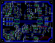
The PCB for the preamp
The PCB layout that I've done so far barely fits everything onto one PCB for both channels. (Remember, I use Eagle's free version, where PCBs cannot exceed 3.2"x4".) It's a single-sided PCB; all red tracks will be executed using jumpers.
")
Tarun
The PCB layout that I've done so far barely fits everything onto one PCB for both channels. (Remember, I use Eagle's free version, where PCBs cannot exceed 3.2"x4".) It's a single-sided PCB; all red tracks will be executed using jumpers.
- It's a single-sided PCB. The top half handles the entire work for the left channel, and the bottom half handles the right.
- It expects clean regulated 15-0-15 (or thereabouts) supply rails. The PSU circuit is not on this PCB.
- There is no separation between power supply ground and signal ground... there's no star grounding. Can't see how I can do it without increasing board size or adding half a dozen or more jumpers.
- All switches and pots are assumed to be panel-mounted, i.e. off-board. Hence, shielded hookup wires are expected to be used for all that wiring. The shields of such hookup wires will need to be grounded. Solder pads have been provided for the worst-case scenario for such wires, i.e. assuming that all your hookup wires are just 1 core+ shield. In reality, it is likely that you'll get 2-cores + shield or 3-cores + shield, in which case you won't need to use all those shield solder-pads. They can be left unused.
Tarun
Attachments
Ouch. I was dreading someone would say this. But I guess I'd better struggle now than get all sorts of problems when I build it.Bill Fitzpatrick said:Personally, I would make every effort to come up with a layout that would allow for separate signal and power grounds.
Tell me, do the shield grounds for the shielded hookup cables qualify as "power" or "signal" ground? I really can't figure this out.
Thanks for the feedback. Anything else you think I should fix?
Tarun
Hi Tarun,
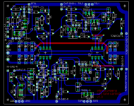
it looks like a small section of the GND trace is going in a complete circle (see the top left corner of the PCB, basically encompassing C1, R3 and Vol1). I''m not sure if this is a good idea, the loop may pick up noise.
Also, I'm a bit surprised that you didn't simply mirror the pattern for one channel to get two. That's what I did for my phono preamp with no problems. Any reason why you didn't do this?
Also, you might want to put slightly bigger values in parallel with C17/C18 for the power supply entry point, maybe 10uF/100uF ? (not sure if this is really required, it's just something I do for my PCBs).
- Ashwin
You're damn right! I fixed it, attached below.ashwin said:it looks like a small section of the GND trace is going in a complete circle (see the top left corner of the PCB, basically encompassing C1, R3 and Vol1). I''m not sure if this is a good idea...
I didn't even know such a thing was possible. It was only during this PCB design that I fully understood how to mark groups and move/cut/paste them. For the schematic layout, I did one channel and then did a group cut/paste to get the other channel, and thought myself totally brilliant. Then I used gateswap to get the unnecessary IC opamps out of the schematic and replace them with spare opamps of the earlier ICs, and considered myself positively Einsteinian. Now you tell me about mirroring of PCB? Sigh...Also, I'm a bit surprised that you didn't simply mirror the pattern for one channel to get two. That's what I did for my phono preamp with no problems.
Will do. Can't harm anything. As long as I can find the board space.Also, you might want to put slightly bigger values in parallel with C17/C18 for the power supply entry point, maybe 10uF/100uF?
Thanks.
Tarun
PS: BTW, if anyone wants these layouts, just ask. I can send you the Eagle directory contents, zipped. Or I can send you PostScript or PDF of track side, component side legends, or solder mask, 1:1 or 1:2. Remember, it's work in progress, so you'll get whatever the current snapshot is. I won't post the files to the forum unless a lot of people ask; send me email.
Attachments

That's exactly the point. I get conflicting views about the need for star grounding in circuits like this. I asked Randy Slone, one of the Gurus I have learned many things from, and he says it's not necessary for signal-level circuits. I asked Angshu, another of my Gurus, and he says that he always does star grounding, even for low-current stuff. Others on this thread seem to have one or other opinion. I don't know what to follow.runebivrin said:Near as I can tell, this circuit has no power ground beyond what goes to the filter caps. There's no low impedance return from a loudspeaker to consider, so currents in the ground should be insignificant.
Tarun
tcpip said:
I didn't even know such a thing was possible. It was only during this PCB design that I fully understood how to mark groups and move/cut/paste them. For the schematic layout, I did one channel and then did a group cut/paste to get the other channel, and thought myself totally brilliant. Then I used gateswap to get the unnecessary IC opamps out of the schematic and replace them with spare opamps of the earlier ICs, and considered myself positively Einsteinian. Now you tell me about mirroring of PCB? Sigh...
Actually, I've never used Eagle, I make my PCBs ye olde manual way
I guess eagle should allow duplication (that's what I meant, not mirroring, silly me..) Basically one opamp per channel, lay out one channel, then copy/paste the whole layout beside itself and connect up the supplies.
- Ashwin
Wow. You're one of those Real Men I keep hearing about. I must meet you when I visit B'lore next.ashwin said:Actually, I've never used Eagle, I make my PCBs ye olde manual way
Aha! Caught you. That wouldn't work if I tried it with the layout approach I was attempting. I wanted to lay out the dual-opamp chips along the centre to get a dividing line, and try to not get signals to cross from one side to another of this line. That way, I thought I could reduce jumper count. However, maybe it's easier just to follow your approach, and I can also reduce crosstalk.I guess eagle should allow duplication (that's what I meant, not mirroring, silly me..) Basically one opamp per channel, lay out one channel, then copy/paste the whole layout beside itself and connect up the supplies.
My dividing-line approach can only be replicated by lateral inversion-mirroring along the dividing line, not general copying.
BTW, I seem to have somehow managed to separate power ground from signal ground. I decided, somewhat arbitrarily, that for a signal-level circuit using opamp chips, the only thing which is "power ground" is the point where the decoupling caps meet, and the ground wire comes from the PSU. Everything else is signal ground. If this assumption is correct, I've managed a separation, and they now connect at just one point, on the right side of the PCB.
Tarun
Attachments
tcpip said:
Wow. You're one of those Real Men I keep hearing about. I must meet you when I visit B'lore next.
Let's do that. Hopefully you'll have some good news on your preamp
Regarding the duplicating thing, I would probably have done it like this: IC1 for one channel, input at the bottom of the board, output at the top, supply at the left-middle of the board. Then copy/paste this to the right of itself.
Anyway, I'm just splitting hairs, I don't see any great advantage either your way or mine.
Do keep us posted.
- Ashwin
Only if you run audio through the shield. If you only connect the shield at one end, it should be connected separately back to the "star" (common) ground or the power ground (it has to drain off the crap it picks up). Running audio through a shield is not recommended; I generally use a different wire to run the input & output connection grounds back to the signal grounds.Bill Fitzpatrick said:The shield grounds are signal grounds.
I know for a fact that I'll have a few interesting people to meet if I land up in B'lore, thanks to this forum. I'll let you know.ashwin said:Let's do that. Hopefully you'll have some good news on your preamp
Yes, that seems like a good idea, and the purist in me keeps feeling that I'm letting myself down on the crosstalk angle by doing both channels in one chip the way I've done. Maybe I'll build this PCB, make a preamp, see how it sounds on other fronts, and then do a v2.0 of the PCB, keeping schematic the same.Regarding the duplicating thing, I would probably have done it like this: IC1 for one channel, input at the bottom of the board, output at the top, supply at the left-middle of the board. Then copy/paste this to the right of itself.
But in your approach, you'll almost certainly need jumpers to take the supply lines across from left-centre to right-side IC for the second channel, right? Not that jumpers are bad or anything, but I just asked. I traded off on those jumpers things when I did the layout the way I did, and I finally landed up jumpering the ground line anyway.
Have found out some interesting resources for chassis and knobs, which other Indian DIYaudio chaps may be interested in. Will post in a separate thread in the Electronics/Parts forum now.
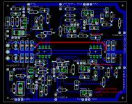
Have now added the large-value cap to the PCB for supply decoupling. How does it look now?
Tarun
Attachments
Can you please explain in a bit more detail? What is the meaning of "running audio through the shield?"paulb said:Only if you run audio through the shield. If you only connect the shield at one end, it should be connected separately back to the "star" (common) ground or the power ground (it has to drain off the crap it picks up). Running audio through a shield is not recommended; I generally use a different wire to run the input & output connection grounds back to the signal grounds.
I'll tell you what I was intending to do. I was going to use 1-core+shield thin hookup wire for the internal wiring in the chassis. I would connect the core of the hookup wire to the inner conductor of the RCA socket at one end, the shield to the outer conductor. At the PCB end, I'd take the inner core to the signal input terminal, and connect the shield to the solder-pad I'm keeping for shield grounding. I was intending to follow this practice for all shielded internal hookup wire.
Does this qualify as "running audio through the shield?"
Sorry, I'm new to all this.
Tarun
tcpip said:
Can you please explain in a bit more detail? What is the meaning of "running audio through the shield?"
I'll tell you what I was intending to do. I was going to use 1-core+shield thin hookup wire for the internal wiring in the chassis. I would connect the core of the hookup wire to the inner conductor of the RCA socket at one end, the shield to the outer conductor. At the PCB end, I'd take the inner core to the signal input terminal, and connect the shield to the solder-pad I'm keeping for shield grounding. I was intending to follow this practice for all shielded internal hookup wire.
Does this qualify as "running audio through the shield?"
Sorry, I'm new to all this.
Tarun
Well, I'm not paulb, but I'll try anyway
Use a cable with 2 cores + 1 sheld. connect one core to the RCA socket's inner conductor, the other core to the RCA socket's outer conductor. The other ends ot the two cores will be connected at the PCB to the signal-in and signal-GND points. The shield must be connected at one end only to the star GND point.
In your method, the signal current would flow from the source to the RCA jack center core, through to the preamp GND, through the shield and back to the source via the RCA jack, completing the loop. The shield thus carries the signal current. I think this is what paulb meant by "running audio through the shield". In my method, the signal current loop is carried by the two cores of the cable and not the shield, because the shield is connected at one end only, so it cannot comlpete any circuit.
My understanding is that grounding the shield at one end creates a capacitance between the core and GND, so that noise capacitively coupled into the core is bypassed to ground through the shield-core capacitance. Grounding the shield at both ends, on the other hand, creates a ground loop. On the third hand
using the shield to carry the audio return current defeats the shield. Here's a link to info on shielding, hum, ground loops etc:
http://www.epanorama.net/documents/groundloop/index.html
Also see fig. 5 in this doc : http://www.rane.com/pdf/groundin.pdf
- Ashwin
Two cores plus shield
Actually, intuitively, I've always felt that two cores plus shield should be the right way to shield any signals, so that both legs of signal carrying conductors are shielded. However, I changed my mind when I saw that RCA-terminated interconnects themselves are just one-core+shield. I then decided that my earlier intuition must've been paranoia.
Thanks again,
Tarun
Thanks. Got it. And if I've understood you right, I don't have to modify my PCB to do the wiring this way. Correct?ashwin said:Use a cable with 2 cores + 1 sheld. connect one core to the RCA socket's inner conductor, the other core to the RCA socket's outer conductor. The other ends ot the two cores will be connected at the PCB to the signal-in and signal-GND points. The shield must be connected at one end only to the star GND point.
Actually, intuitively, I've always felt that two cores plus shield should be the right way to shield any signals, so that both legs of signal carrying conductors are shielded. However, I changed my mind when I saw that RCA-terminated interconnects themselves are just one-core+shield. I then decided that my earlier intuition must've been paranoia.
Thanks again,
Tarun
I am not sure I have been able to understand your point accurately, but it seems to me to be very similar to a doubt I had about the very same junction. I wrote to Randy Slone (Sat 13 July 2002; I still have my email and his reply). My doubt basically was the following: purely going by symmetry of the topology, it seemed to me that the left sides of R15, C6, and C7 should connect to each other, but the right side of R10 should not connect to this junction. The right side of R10 should connect straight to the E-terminal of MID-L, just like the right side of R9 connects straight to the E-terminal of BASS-L, and so on.Bo Hansén said:I notice a drawing fault in your schematic, maybee you already have find this missing in the mid eq section.
R10 shall only go to C10 and the mid. potentiometers "E" terminal, and not together with C6, C7.Those shall go to R15, C9 and pin 6 on IC2B.
Randy answered me, saying that he understood what I was saying, but the schematic in his book was correct, and this asymmetry is intentional. His words were "The Fig 4.1 schematic is correct. The departure between it and Fig 3.7 is just a slightly different design -- I feel that the Figure 4.1 design provides a little better overall response." (All these Figure numbers are of course with reference to his book, Audiophile projects sourcebook.)
That was that. I wish I knew how to simulate circuits and their frequency responses. If you can, will you please check? And first of all, are we both talking about the same confusion?
Tarun
- Status
- This old topic is closed. If you want to reopen this topic, contact a moderator using the "Report Post" button.
- Home
- Amplifiers
- Solid State
- A preamp with tone controls