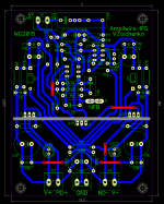
I guessed right on the resistor wattages. I've got the schematic drawn. I should have a board done later today.
Wow!
 Cool
Cool Actually - as an option - 1W resistors can be SMD 2512 under the board - small, easy to solder, good heat dissipation... still single-sided
This thought flew through my mind at some point, but I decided to pretend it's no problem Never had any damages though...
Ah! One more thing. Let's put a couple of additional connectors, so that one can drop 6.8k 1W resistors and zeners, and connect the IPS section to standalone +/-15V regulated power supply. For "hi-end" builds
Never had any damages though...Ah! One more thing. Let's put a couple of additional connectors, so that one can drop 6.8k 1W resistors and zeners, and connect the IPS section to standalone +/-15V regulated power supply. For "hi-end" builds
Is R1 and R3 going to be okay at 1/4W?
yes - low voltage and rather low current...
(1.8V - 0.65V) * 5.35 mA = 6 mW per resistor
OS's Jung regulator would be a great addition to this board. I'll add the connector for it in the double sided version. Would there be any advantage to adding ground lift diodes as we do in the Slewmasters?
yes, the diodes will be a valid addition as well

OS's Jung regulator - yep, cool. This one is going to be a very low noise IPS - 2N5089 are great devices - I easily had around -120db at my previous prototype with them.
I've never seen those 2N5089's before. Are they a big advantage over the BC5xx?
I've never seen those 2N5089's before. Are they a big advantage over the BC5xx?
high gain and low noise at the same time... yes, even better noise characteristic than BC5xx
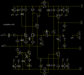
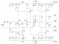
Here is my vision....Ground star and input section as compact as i could ...
Marc
Hi Marc - cool version. One thing - middle (moving) and bottom pins of TR5 pot should be connected.

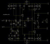
Variation with MOSFET as a VAS core
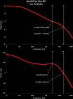
Just tried an interesting option with IRF9610 as a VAS core.
Around 10db higher loop gain, a bit sharper square wave response.
Although - very close to the original version.
It can be built on the same PCB - just the FET needs to be flipped over:
BJT pinout is ECB;
FET pinout is GDS - after flipping over it will be SDG - just what we need.
I have also added an optional C9 (1pF) cap from the VAS output to NFB side input (negative) - it would be good to add it to the PCB for either option.
All the values, different from the original design, are shown in RED. Sorry for an accidental RefDes "renumbering" - this illustration is just to show a few value differences.
Keeping in mind overall simplicity of the design, it would be interesting to see if somebody will notice some audible difference between those BJT/FET VAS options in a proper A/B test
Attachments
Would there be any advantage to using fets for Q2 and Q7?
I don't think so, although I will try to sim it as well.
- Home
- Amplifiers
- Solid State
- Revisiting some "old" ideas from 1970's - IPS, OPS