current-driven
Hi Valery,
That's a very good idea, though our implementations are quite different.
Cheers, E.
Hello All,
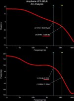
I continued thinking about the ways of making the VAS faster, more linear, keeping it stable at the same time. At some point, an idea came in - why don't I try to arrange the VAS stage in such a way, that it's somewhat "current-driven"?
[...]
Cheers,
Valery
Hi Valery,
That's a very good idea, though our implementations are quite different.
Cheers, E.
Hi Valery,
That's a very good idea, though our implementations are quite different.
Cheers, E.
Hi Edmond,
Thank you for the feedback
") Trying to keep it "pure" and simple at the moment. Although, I see many directions for further development, based on this principle
Trying to keep it "pure" and simple at the moment. Although, I see many directions for further development, based on this principle Cheers,
Valery
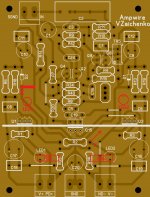
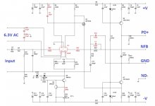
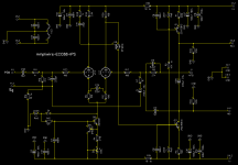
Just tried an interesting option with IRF9610 as a VAS core.
Around 10db higher loop gain, a bit sharper square wave response.
Although - very close to the original version.
It can be built on the same PCB - just the FET needs to be flipped over:
BJT pinout is ECB;
FET pinout is GDS - after flipping over it will be SDG - just what we need.
I have also added an optional C9 (1pF) cap from the VAS output to NFB side input (negative) - it would be good to add it to the PCB for either option.
All the values, different from the original design, are shown in RED. Sorry for an accidental RefDes "renumbering" - this illustration is just to show a few value differences.
Keeping in mind overall simplicity of the design, it would be interesting to see if somebody will notice some audible difference between those BJT/FET VAS options in a proper A/B test
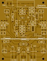
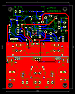
I tried my hand at following Marc's layout in Sprint. I added C19 and a place to use a FET in place of Q15. If youhave a chance would you look it over and see if I have it right?
Thanks, Terry
Attachments
I tried my hand at following Marc's layout in Sprint. I added C19 and a place to use a FET in place of Q15. If youhave a chance would you look it over and see if I have it right?
Thanks, Terry
Hi Terry, in this case I would move the LEDs and turn R35, R36 90 degrees, making the bottom area even less "busy" and saving one jumper wire (vertical, near R36). Cool variant

Attachments
Hi Terry, in this case I would move the LEDs and turn R35, R36 90 degrees, making the bottom area even less "busy" and saving one jumper wire (vertical, near R36). Cool variant
Nice tricks....
Marc
Attachments
Last edited:
This will be more useful if you can post pdf or jpeg(diy friendly)Following Valery new suggestions
Last edited:
And finally... Tubie
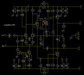
Rather simple hybrid with 6DJ8 tube at the input.
Interesting to hear the prototype. Same high open loop linearity, rather fast.
Which one will show less noise - the one with low noise BJTs or the one with the tube at the input?
It will work fine with the rails from +/-35V to +/-75V (with possible adjustment of R7, R24).
OK, I will stop here Let's build and see (and hear)
Marc has already got a draft layout for this one as well
Rather simple hybrid with 6DJ8 tube at the input.
Interesting to hear the prototype. Same high open loop linearity, rather fast.
Which one will show less noise - the one with low noise BJTs or the one with the tube at the input?
It will work fine with the rails from +/-35V to +/-75V (with possible adjustment of R7, R24).
OK, I will stop here
Let's build and see (and hear) Marc has already got a draft layout for this one as well
Attachments
This will be more useful if you can post pdf or jpeg(diy friendly)
Hi thimios. It's a Jpeg file. If some one want file to make board feel free to ask.
Marc
Edit : i just see that files are not Jpeg but PNG....even PNG is a picture file type..
Last edited:
Hi thimios. It's a Jpeg file. If some one want file to make board feel free to ask.
Marc
I think he's asking for separate pictures for copper and silk so he can use them to etch a board from. PDF files make much smoother trace lines for home etching.
I think he's asking for separate pictures for copper and silk so he can use them to etch a board from. PDF files make much smoother trace lines for home etching.
If some one want file to etch board he may ask me as it depend on way to do the etching. Every time i done routing job i share work if some show interest no issue with that. At this step in this topic work is evoluting and may be not final.
Marc
Rather simple hybrid with 6DJ8 tube at the input.
Interesting to hear the prototype. Same high open loop linearity, rather fast.
Which one will show less noise - the one with low noise BJTs or the one with the tube at the input?
It will work fine with the rails from +/-35V to +/-75V (with possible adjustment of R7, R24).
OK, I will stop here
Marc has already got a draft layout for this one as well
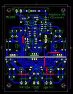
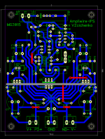
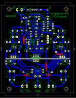
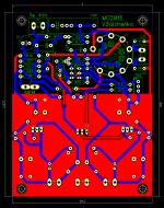
Here it is :
Schematic
top layer
Botton Layer
I will try if i can made one layer PCB...
Attachments
Following Valery new suggestions
I have a question about the layout. Why is it better to have several small ground traces running parallel to each other rather than just ganging them together into one larger trace?
Thanks, Terry
It's better to bring each part of the circuit back to a central point so noise from one part won't effect the next circuit as much. I usually bring complete parts of a circuit back if possible. For example if there's a zener regulating a circuit, I would bring the ground from it back with it's following capacitors. All input lifted grounds would come back together, ect.
I think he's asking for separate pictures for copper and silk so he can use them to etch a board from.I think he's asking for separate pictures for copper and silk so he can use them to etch a board from. PDF files make much smoother trace lines for home etching.
Exactly,thanks Jeff.
It's better to bring each part of the circuit back to a central point so noise from one part won't effect the next circuit as much. I usually bring complete parts of a circuit back if possible. For example if there's a zener regulating a circuit, I would bring the ground from it back with it's following capacitors. All input lifted grounds would come back together, ect.
Exactly. It also makes sense to group the ground traces in a way that you isolate relatively high-power areas from the low-power ones (as high-power ones may have some ripple, the longer the trace is - the higher the ripple is).
But a zener and a couple of capacitors can easily be ganged together, as those capacitors - both filter the rail and reduce the noise from that zener.
I think he's asking for separate pictures for copper and silk so he can use them to etch a board from.
Exactly,thanks Jeff.
So let me know exatly what you need : mirror....etc
Marc
- Home
- Amplifiers
- Solid State
- Revisiting some "old" ideas from 1970's - IPS, OPS