Hi Federico,
Thank you for giving the formula and the parameters.
I see two problems with using this formula for FETS
a) I'll guess IDS/VDS => 0 as VDS => 0. In the FET this should have a non-zero limes.
b) the square law isn't a square law
Nevertheless the pragmatic fitting is great!
The level 1 FET model just stitches three different functions together, if using instead a continuous blending function like atan, things would looks nicer. But I'll have to read more about higher level FET models to see if anything there can be re-used for JFETs.
Regards,
Peter Jacobi
fscarpa58 said:It is the classic pentode model slightly modified
to account for the square law of FETs.
Thank you for giving the formula and the parameters.
I see two problems with using this formula for FETS
a) I'll guess IDS/VDS => 0 as VDS => 0. In the FET this should have a non-zero limes.
b) the square law isn't a square law
Nevertheless the pragmatic fitting is great!
The level 1 FET model just stitches three different functions together, if using instead a continuous blending function like atan, things would looks nicer. But I'll have to read more about higher level FET models to see if anything there can be re-used for JFETs.
Regards,
Peter Jacobi
a) I'll guess IDS/VDS => 0 as VDS => 0. In the FET this should have a non-zero limes.
b) the square law isn't a square law
Hi
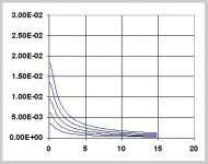
I just tried, IDS/VDS has a finite, non-zero, limit if VDS tends to zero as you can see in the attached pic.
Regarding the square law the problem
can be faced by using the variant from
Koren.
regards
Federico
Attachments
Peter, sorry, I do not have that book so can not know what you are referring to. Curve matches to the datasheet (below) very well, that is why I posted it. Many models are doing here just fine.pjacobi said:Compare formulas 3-11 and 3-12 in Massobrio/Antognetti. And the datasheet curves.
I am interested in SPICE only like a user, but generally I would sayfscarpa58 said:I think spice model developers
have to work more and better.
Any comment ?
 .
.And comment on the findings you posted is: excellent work!
Slightly out of topic, but one parallel with bjt models: similarly to JFETs, many of them have wrong (too good) Ic/Vce characteristic and I guess this is (one of) the reason why harmonic distortion often looks lower in the simulators than in the real world. Well modeled hFE/Ic is also rather exception than rule.
Pedja
Attachments
II agree with your statement about
BJT, Pedja ( and thanks for your appreciation).
However I have to admit my ignorance
about this subject. BJT modeling is more
difficult for me owing to the presence of a
significant base current.
So, I feel more familiar with tubes and FETs.
Regarding tubes, I have to say that models are, in
general, quite good (at least using Koren approach).
I always observed great correlation between the
real distortion spectrum and the simulated one.
Regarding the analysis of the ID versus VGS curves, I think
(my opinion) that it is not a good way to judge
a model. The ID vs. VDS curves are
a better one.
Regards,
Federico
Hi Federico, Pedja, Christer, Lurkers,
Had some day work to do, so that I can't fully address all topics raised so far. So only some short comments:
*** a) Pentode model adapted for JFETs ***
If this is the homegrown JFET model contest, where shall we send the entries to, and what's the price?
For a direct comparison of the SPICE level 1 model, and two alternatives which smoothly interpolate, look at this deck:
* JFET models
V1 D 0 0
V2 G 0 0
B1 0 D I=12m*2/pi*atan(pi/4*V(D,0)/(V(G,0)/3.9+1.0))*(V(G,0)/3.9+1.0)**2*(V(D,0)+200)/200
B2 0 D I=12m*tanh(0.5*V(D,0)/(V(G,0)/3.9+1.0))*(V(G,0)/3.9+1.0)**2*(V(D,0)+200)/200
B3 0 D I=12m*(V(D,0)+200)/200*if(V(D,0)<V(G,0)+3.9,V(D,0)/3.9*(2*(V(G,0)/3.9+1)-V(D,0)/3.9),(V(G,0)/3.9+1.0)**2)
.dc V1 0 24 10m V2 0 -3 -1
.end
B1 is SPICE level1, B3 is much like the pentode, B2 is another interpolation nearer to B1. All matched to coincede for VDS=>0 and VDS=>inf.
This is for a JFET with VGSoff=3.9V, IDSS=12mA and pseudo-Early voltage of 200V (some similarity with BF556B).
*** b) square law or not ***
(3-11 and 3-12 in Massobrio/Antognetti)
3-12: IDS = IDSS * (1 - VGS/VGSoff)**2
Set
VGSoff = V0 + PHI0
X = (PHI0 - VGS) / VGSoff
3-11: IDS = C * (1 - 3*X + 2*X**1.5)
3-12 is a reasonable approximation to 3-11, especially when VGSoff is smaller than 2...3 * PHI0.
I'll have to double check the formulas, do some curve plotting and re-activate my TeX skills to give a better presentation of this.
*** c) BJT modeling ***
Just learned that there is a differentation operator available in LTSpice curve plotting (D), so that's easy to do hfe/Ic plots.
Yes, most models look really ugly. The few LEVEL 2 models I have access to, look much better. I don't think you can do 2SB649/2SD669 in LEVEL 1.
But, whatever, simply let's use all our BJTs in the constant hfe region! I'll suppose it will sound better.
Regards,
Peter Jacobi
Can't make a single post without a typo or number confusion...
B3 is SPICE level1,
B1 is much like the pentode,
B2 is another interpolation nearer to B3.
Also note that the 0-node is the S-node.
pjacobi said:B1 0 D I=12m*2/pi*atan(pi/4*V(D,0)/(V(G,0)/3.9+1.0))*(V(G,0)/3.9+1.0)**2*(V(D,0)+200)/200
B2 0 D I=12m*tanh(0.5*V(D,0)/(V(G,0)/3.9+1.0))*(V(G,0)/3.9+1.0)**2*(V(D,0)+200)/200
B3 0 D I=12m*(V(D,0)+200)/200*if(V(D,0)<V(G,0)+3.9,V(D,0)/3.9*(2*(V(G,0)/3.9+1)-V(D,0)/3.9),(V(G,0)/3.9+1.0)**2)
.dc V1 0 24 10m V2 0 -3 -1
.end
B1 is SPICE level1, B3 is much like the pentode, B2 is another interpolation nearer to B1.
B3 is SPICE level1,
B1 is much like the pentode,
B2 is another interpolation nearer to B3.
Also note that the 0-node is the S-node.
Peter, others,
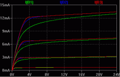
For probably easiest check, MicoCap (there is a free demo) from version 7 has that nice possibility to show a few plots for any used component and for BJTs this includes hFE vs. Ic plots.
For possibly better overview, attached (zipped) MicroCap’s .cir file (done for version 6, normally works in 7) plots these curves for both NPN and PNP device in one page.
Pedja
Attachments
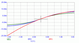
Hi, Pedja, All
Thinking at a given IC as to a working point, if the small signal current gain is required,
is it not better to plot the local derivatives of IC in respect with IB as a function of IC?
The plots are slightly different from your's
Bye
Federico
Thinking at a given IC as to a working point, if the small signal current gain is required,
is it not better to plot the local derivatives of IC in respect with IB as a function of IC?
The plots are slightly different from your's
Bye
Federico
Attachments
Hi Federico,fscarpa58 said:Thinking at a given IC as to a working point, if the small signal current gain is required,
is it not better to plot the local derivatives of IC in respect with IB as a function of IC?
Yes, that is interesting difference to think about. Probably those graphs that show local derivatives might be even more important for the real applications. But I think what we have in the datasheets and what could be the reference for model check is still only the plain Ic/Ib relation in the term of the established currents.
But nice addition to the file, I appreciate.
Pedja
Towards more accurate JFET modeling + Tools question
See also the graph in #23
http://www.diyaudio.com/forums/showthread.php?postid=318580#post318580
By symmetry (if this is a symmetric JFET, but the essentials should also hold for unsymmetrical ones), we should have:
IDS (VGS, VDS) = -IDS (VGS - VDS, -VDS)
and not
IDS (VGS, VDS) = -IDS (VGS, -VDS)
This implies, that the second derivative of IDS in the VDS=>IDS isn't zero. So, the 'crude' Spice Level 1 model (in B3) is right, and the more elegant looking atan or tanh functions are wrong in this aspect. You can (bareley) see it by plotting for VDS=-0.3..0.3V
Some JFET datasheets have a good plot of the low VDS region, where you see this too. In the moment, I'm totally messed up with datasheets flying around, so I can give you concrete references only later.
BTW, can anybody volunteer a (free) tool for doing all the calcs and plotting?
With the help of the LTSpice mailing list (which mostly, and correctly, said 'read the fine online help'), I got my LTSpice experiments less messy. Nevertheless it looks like the wrong tool.
In the past I played a lot with Excel, but this wasn't very satifying.
I now tried (again) to get myself comfortable with SciLab (http://scilabsoft.inria.fr/).
Suggestions?
Peter
pjacobi said:[...]
* JFET models
V1 D 0 0
V2 G 0 0
B1 0 D I=12m*2/pi*atan(pi/4*V(D,0)/(V(G,0)/3.9+1.0))*(V(G,0)/3.9+1.0)**2*(V(D,0)+200)/200
B2 0 D I=12m*tanh(0.5*V(D,0)/(V(G,0)/3.9+1.0))*(V(G,0)/3.9+1.0)**2*(V(D,0)+200)/200
B3 0 D I=12m*(V(D,0)+200)/200*if(V(D,0)<V(G,0)+3.9,V(D,0)/3.9*(2*(V(G,0)/3.9+1)-V(D,0)/3.9),(V(G,0)/3.9+1.0)**2)
.dc V1 0 24 10m V2 0 -3 -1
.end
[...]
See also the graph in #23
http://www.diyaudio.com/forums/showthread.php?postid=318580#post318580
By symmetry (if this is a symmetric JFET, but the essentials should also hold for unsymmetrical ones), we should have:
IDS (VGS, VDS) = -IDS (VGS - VDS, -VDS)
and not
IDS (VGS, VDS) = -IDS (VGS, -VDS)
This implies, that the second derivative of IDS in the VDS=>IDS isn't zero. So, the 'crude' Spice Level 1 model (in B3) is right, and the more elegant looking atan or tanh functions are wrong in this aspect. You can (bareley) see it by plotting for VDS=-0.3..0.3V
Some JFET datasheets have a good plot of the low VDS region, where you see this too. In the moment, I'm totally messed up with datasheets flying around, so I can give you concrete references only later.
BTW, can anybody volunteer a (free) tool for doing all the calcs and plotting?
With the help of the LTSpice mailing list (which mostly, and correctly, said 'read the fine online help'), I got my LTSpice experiments less messy. Nevertheless it looks like the wrong tool.
In the past I played a lot with Excel, but this wasn't very satifying.
I now tried (again) to get myself comfortable with SciLab (http://scilabsoft.inria.fr/).
Suggestions?
Peter
pjacobi said:So, the 'crude' Spice Level 1 model (in B3) is right, and the more elegant looking atan or tanh functions are wrong in this aspect. You can (bareley) see it by plotting for VDS=-0.3..0.3V
Some JFET datasheets have a good plot of the low VDS region, where you see this too. In the moment, I'm totally messed up with datasheets flying around, so I can give you concrete references only later.
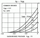
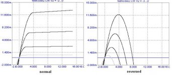
Peter, are you sure about this? If you know any datasheet that shows the curve for negative Vds it will be really a great reference now.
For those who won’t plot that, attached graph shows what Peter is talking about, so if anyone has any idea… As far as I can remember drain and source of JFETs are mostly interchangeable, so what is right and what is wrong here?
With the help of the LTSpice mailing list (which mostly, and correctly, said 'read the fine online help'), I got my LTSpice experiments less messy. Nevertheless it looks like the wrong tool.
I am not sure, what is a problem with it?
Pedja
Attachments
Pedja said:Peter, are you sure about this? If you know any datasheet that shows the curve for negative Vds it will be really a great reference now.
I don't know a datasheet which shows the negative Vds region, but for symmetric JFETs, e.g. the Fairchild 2N5484 series, you can always relabel S<->D, to get the values for negative Vds, using the formula above.
A datasheet, where with the help of a ruler, you can see that d²Id/dVds² stays rather constant when Vds => 0, is Vishay J/SST111 series.
But of course, unless you are really using a JFET with current flowing both ways, the numerical deviation is rather small. Just perfectionism (a.k.a. not-picking) at work.
Regards,
Peter Jacobi
some people do put the current thru the fet both ways:
http://www.qsl.net/n4xy/PDFs/Semico...otes/Vishay-Silcnx_FET_VoltCntrlRES_AN105.pdf
http://www.qsl.net/n4xy/PDFs/Semico...otes/Vishay-Silcnx_FET_VoltCntrlRES_AN105.pdf
Hi Peter, All
I agree with this relation but I use to put it in a more manageable ( for me) manner that is
IDS (VGS, VGD) = -IDS (VGD, VGS)
In other words, we have to solve the functional equation
F(x,y)=- F(y,x)
Referring to model B3, I note that if I turn over (top-down) the device I do not obtain similar curves. ( I plot current by using
a little (1u) res. on the top of the device to avoid sign proiblem)
federico
IDS (VGS, VDS) = -IDS (VGS - VDS, -VDS)
I agree with this relation but I use to put it in a more manageable ( for me) manner that is
IDS (VGS, VGD) = -IDS (VGD, VGS)
In other words, we have to solve the functional equation
F(x,y)=- F(y,x)
Referring to model B3, I note that if I turn over (top-down) the device I do not obtain similar curves. ( I plot current by using
a little (1u) res. on the top of the device to avoid sign proiblem)
federico
Attachments
jcx said:some people do put the current thru the fet both ways:
http://www.qsl.net/n4xy/PDFs/Semico...otes/Vishay-Silcnx_FET_VoltCntrlRES_AN105.pdf
And fig 2 in this nice paper shows the non-vanisching second derivative at the origin very clearly.
fscarpa58 said:I agree with this relation but I use to put it in a more manageable ( for me) manner that is
IDS (VGS, VGD) = -IDS (VGD, VGS)
In other words, we have to solve the functional equation
F(x,y)=- F(y,x)
I agree. Putting it this way, it's much easier to visualize, what the fuction should look like.
fscarpa58 said:Referring to model B3, I note that if I turn over (top-down) the device I do not obtain similar curves. ( I plot current by using
a little (1u) res. on the top of the device to avoid sign proiblem)
This looks fine already for the non-saturated region. Should be tweakable for a solution in the complete plane.
Other points to note:
The 2004-02-09 version of LTSpice did get the MESFET working. It's Statz' model (LEVEL 1 in AIMSpice, LEVEL 2 in PSPICE).
Not checked everything, but would also be nice to use for JFETs.
Main differences to JFET LEVEL 1
Uses 1 - (1 - x**3) instead of 1 - (1 - x**2) to interpolate between linear and saturated region.
Has an additional parameter for VGS=>VDS which allows to model the transfer characteric of devices which higher VGSoff, which approach linear near 0 VGS.
Regards,
Peter Jacobi
- Status
- This old topic is closed. If you want to reopen this topic, contact a moderator using the "Report Post" button.
- Home
- Amplifiers
- Solid State
- Borbely Fet Follower SPICE modeling