Amp designed during lunch breaks (The Lunch-Break Amp)
Hi All,
Decided that as I waste most of my time during lunch breaks at work decided it might be a good idea to install LTSpice and design amps instead. Well here is the result so far.
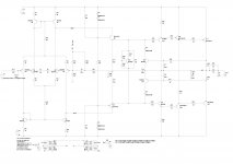
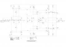
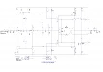
It is a simplified Super TIS (by Edmond Stewart) front end with some OIC MI compensation (I think) and non error corrected OPS.
The output inductor values and vbe multiplier component values are guessed at present. Also, decoupling has been ommitted for clarity of schematic.
Here is the schematic along with the latest .asc
Edit: Latest .asc now here http://www.diyaudio.com/forums/solid-state/265449-amp-designed-during-lunch-breaks-14.html#post4246674
Paul
Edit: Loop analysis tools provided by David Zan.
Hi All,
Decided that as I waste most of my time during lunch breaks at work decided it might be a good idea to install LTSpice and design amps instead. Well here is the result so far.
It is a simplified Super TIS (by Edmond Stewart) front end with some OIC MI compensation (I think) and non error corrected OPS.
The output inductor values and vbe multiplier component values are guessed at present. Also, decoupling has been ommitted for clarity of schematic.
Here is the schematic along with the latest .asc
Edit: Latest .asc now here http://www.diyaudio.com/forums/solid-state/265449-amp-designed-during-lunch-breaks-14.html#post4246674
Paul
Edit: Loop analysis tools provided by David Zan.
Attachments
Last edited:
Long lunch breaks
")
You know they are.
looks very promising!
Thank you.
Hopefully... It will be a lot more promising once a strip board prototype has been built.
There is still some development to go. Been concentrating on loop stability up till now. Today's lunch break will be the start of working out better SOA protection for the output stage.
Probably go for a dual slope.Paul
Hopefully... It will be a lot more promising once a strip board prototype has been built.
There is still some development to go...
in my sims I found strong oscillations @~10MHz but maybe because it was only more or less rough schematic/idea or different models (I use cordell-models.txt)

in my sims I found strong oscillations @~10MHz but maybe because it was only more or less rough schematic/idea or different models (I use cordell-models.txt)
Interesting...
I too use Cordell models and where necessary in built LTSpice models.
How did you manage to get this amp to oscillate? I'm still only really a beginner (/ improver
) with amplifier design. Thank you for taking the time to have a look at my amp.
...delet[e] the loop analysis tools. There is some sort of interaction
Hey, the tools are fine.
Your Ltspice has an error, there is no .SET statement.
The correct syntax is
.Param Tn=0 Tm=0
Best wishes
David
The tools are the best. It's the user in this case...Hey, the tools are fine.
Have I got the placement correct?
Your Ltspice has an error, there is no .SET statement.
The correct syntax is
.Param Tn=0 Tm=0
Best wishes
David
And the most embarrassing bit for me is that we discussed this not so long ago with Damir.
Will add the correction. Thank you for pointing this out (again).
There will be an update on this project soon. Got new values for the Thiele / Cherry output network.
Paul
Last edited:
...the placement correct?
Not quite for the Zan/Z0 nodes, I suspect. Just back from a few days in Syn city (Sydney) so a bit tired, always lots of posts while I am otherwise occupied
But I think you need to check the outer loop with a probe from the junction of R13 - R14 to the bases of the input transistors Q3 and Q4.
Your probe position for Edmond's cascode VAS looks correct but I have never checked that particular circuit so will think a bit more to be sure.
Best wishes
David
Not quite for the Zan/Z0 nodes, I suspect. Just back from a few days in Syn city (Sydney) so a bit tired, always lots of posts while I am otherwise occupied
Syn City
Always the way, there is never enough time for life, diyaudio and sleep.
But I think you need to check the outer loop with a probe from the junction of R13 - R14 to the bases of the input transistors Q3 and Q4.
Your probe position for Edmond's cascode VAS looks correct but I have never checked that particular circuit so will think a bit more to be sure.
Best wishes
David
Will have a think about your suggestion for Zan/Zo. The compensation is like TMC but with MIC front end and OI back end. It appears to work but only marginally better than a cap across the feedback resistor. So maybe I do have the probe placement wrong.
Go get some rest.
Paul
Last edited:
Not quite for the Zan/Z0 nodes...
...But I think you need to check the outer loop with a probe from the junction of R13 - R14 to the bases of the input transistors Q3 and Q4.
Best wishes
David
Been looking at this. Looks like you can analyse this with one probe placed where you suggest above. This would also stimulate the VAS due to the type of compensation.
(Now I prepare to be corrected
)Paul
...Looks like you can analyse this with one probe.... This would also stimulate the VAS due to the type of compensation.
Looks correct to me.
The simple probe placed where I recommended, at the bases of the input transistors, should return essentially the same result as the differential probe where you already have it, for the VAS, with the compensation you have.
This will be a useful cross-check, which I claim as my excuse for why I didn't immediately see this last nite.
Exactly what to call the compensation is a bit less clear.
I don't see it as close to TMC (not "transitional") or OIC (which I define as Miller compensation from the OPS back to the VAS).
It is a Two Pole (to use the term loosely) overall loop with some shunt compensation.
Best wishes
David
Last edited:
Looks correct to me.
The simple probe placed where I recommended, at the bases of the input transistors, should return essentially the same result as the differential probe where you already have it, for the VAS, with the compensation you have.
This will be a useful cross-check, which I claim as my excuse for why I didn't immediately see this last nite.
Well the cross check was done last night. The simple and differential probes produced virtually the same result out in to the 50MHz region then things diverged. Maybe this is where the GFT would be useful.
Exactly what to call the compensation is a bit less clear.
I don't see it as close to TMC (not "transitional") or OIC (which I define as Miller compensation from the OPS back to the VAS).
It is a Two Pole (to use the term loosely) overall loop with some shunt compensation.
Best wishes
David
Good question... What to call it...
It almost certainly isn't worth having two pole comp for the main loop. It makes almost no difference to performance or stability. Think it cost 2ppm @ 20kHz.
When I rearranged the schematic to show all the feedback paths from the OPS to the IPS. It all became clearer and really isn't TMC. All it is some lead/lag + lead across the feedback resistor, along with some shunt comp @VAS output.
Have managed to get it working with just plain shunt caps @ the VAS output and resistor + cap across the feedback resistor.
Not so confident with this amp. It looks deceptively simple... Prototype will tell.
Paul
Hello all,
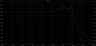
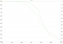
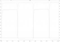
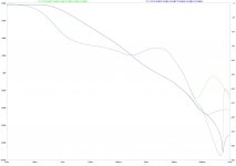
Here is the next iteration. It sims ok. Maybe this should be the prototype. I am a little concerned at the high ULGF. The amp seems to want to run fast. If you slow it down all the compensation looks sub-optimal. Stability margins look ok to me. Can get better PM by increasing the ULGF but at the expense of GM.
What do people think? All opinions are greatly valued.
Padamiecki
Attachments:
1) .asc for anyone interested in this madness.
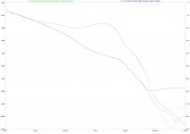
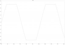
2) Schematic
3) Current Limit into 0.1R with output network bypassed.
4) Stability plots
Are my attachments readable for you guys?
Paul
Here is the next iteration. It sims ok. Maybe this should be the prototype. I am a little concerned at the high ULGF. The amp seems to want to run fast. If you slow it down all the compensation looks sub-optimal. Stability margins look ok to me. Can get better PM by increasing the ULGF but at the expense of GM.
What do people think? All opinions are greatly valued.
Padamiecki
Attachments:
1) .asc for anyone interested in this madness.
2) Schematic
3) Current Limit into 0.1R with output network bypassed.
4) Stability plots
Are my attachments readable for you guys?
Paul
Attachments
Hello all,
Here is the next iteration. It sims ok. Maybe this should be the prototype. I am a little concerned at the high ULGF. The amp seems to want to run fast. If you slow it down all the compensation looks sub-optimal. Stability margins look ok to me. Can get better PM by increasing the ULGF but at the expense of GM.
What do people think? All opinions are greatly valued.
Padamiecki
Attachments:
1) .asc for anyone interested in this madness.
2) Schematic
3) Current Limit into 0.1R with output network bypassed.
4) Stability plots
Are my attachments readable for you guys?
Paul
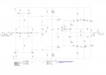
No, not very readable. I don't like when a schematic or a plot expand outside my screen, and why you don't use a grid?
No, not very readable. I don't like when a schematic or a plot expand outside my screen, and why you don't use a grid?
Lets start with the schematic... It's now smaller but not very legiable.
I see it as I'm asking for the help and the good nature of people on this site. Just want to make it easy for them.
Attachments
Last edited:
Lets start with the schematic... It's now smaller but not very legiable.
I see it as I'm asking for the help and the good nature of people on this site. Just want to make it easy for them.
Still to big, or my screen is to small (I use a laptop) or your (screen) is to big.
- Status
- This old topic is closed. If you want to reopen this topic, contact a moderator using the "Report Post" button.
- Home
- Amplifiers
- Solid State
- Amp designed during lunch breaks