edit 20-Jul-2014.
See post #38 for ANUBIS final schematic and the power supply design.
Hi,
Just finished building this but i haven't flipped the power switch ON.
The reason being that i'm not sure if this contraption i designed would work. I have personally gone through the schematic many times and can't see anything wrong with it.. but i can very well be wrong.
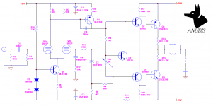
If anyone can check the schematic for any fatal error before i end up with burned transistors, it would be great. So.. here's Another Tube Transistor Hybrid Amp.. or ANUBIS for short.
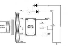
The basic idea is simple: take a working solid state power amplifier design and replace the input stage with tube. The topology is very common: Long Tailed Pair --> Class A VAS --> Compound Pair output. Have Rod Elliot's P3A PCB lying around? With some minor modification and creativity, you can use it for ANUBIS. For fellow Indonesians, our ubiquitous "150-300W OCL Amplifier" PCBs can also be used. I have also attached the Power Supply Design i use.
These are the stuff that i'm still not sure about ANUBIS:
1. VAS Class A stage, especially whether R8 and R9 values are correct. I tried to aim at 10-11mA of idle collector current. Can anyone show me the correct calculation for R8 and R9?
2. Will there be problem at cold starts? I mean when first turning on and the tube has not warmed up (and conducted) yet. I use DC protection for the speaker so temporary high offset is ok. I'm just not sure if the transistors will survive.
3. Will there too much voltage offset at the output?
note: i've created similar thread in the Tube forum but decided since i'm basing this off a working SS amp, it should be here. I will ask mods to delete my thread there.
See post #38 for ANUBIS final schematic and the power supply design.
Hi,
Just finished building this but i haven't flipped the power switch ON.
The reason being that i'm not sure if this contraption i designed would work. I have personally gone through the schematic many times and can't see anything wrong with it.. but i can very well be wrong.
If anyone can check the schematic for any fatal error before i end up with burned transistors, it would be great. So.. here's Another Tube Transistor Hybrid Amp.. or ANUBIS for short.
An externally hosted image should be here but it was not working when we last tested it.
The basic idea is simple: take a working solid state power amplifier design and replace the input stage with tube. The topology is very common: Long Tailed Pair --> Class A VAS --> Compound Pair output. Have Rod Elliot's P3A PCB lying around? With some minor modification and creativity, you can use it for ANUBIS. For fellow Indonesians, our ubiquitous "150-300W OCL Amplifier" PCBs can also be used. I have also attached the Power Supply Design i use.
These are the stuff that i'm still not sure about ANUBIS:
1. VAS Class A stage, especially whether R8 and R9 values are correct. I tried to aim at 10-11mA of idle collector current. Can anyone show me the correct calculation for R8 and R9?
2. Will there be problem at cold starts? I mean when first turning on and the tube has not warmed up (and conducted) yet. I use DC protection for the speaker so temporary high offset is ok. I'm just not sure if the transistors will survive.
3. Will there too much voltage offset at the output?
note: i've created similar thread in the Tube forum but decided since i'm basing this off a working SS amp, it should be here. I will ask mods to delete my thread there.
Attachments
Last edited:
Member
Joined 2009
Paid Member
Great - I love to see the interest in hybrids these days. Just a very quick look - careful about power dissipation and voltage rating for the VAS device since it hangs off the B+ rail and will swing as far negative as the signal itself. You might be able to reduce your B+ as these tubes are usually known to be good for lower voltages.
Also be careful of turn-on/off behaviour as tubes warm up.
Also be careful of turn-on/off behaviour as tubes warm up.
- Emitter of Q2 should connect to collector of Q4 and emitter of Q3 should connect to collector of Q5 for stability, not to output
- Q7 should be bolted on the heatsink along with Q2-Q5 for thermal compensation
- There should be a 100-220pF capacitor from base to Collector of Q3 to prevent oscillation
- A 1A diode in series with ~10 R should connect collector of Q1 to protect SS section during power on/off and input section malfunction
- Heater of V1 should be on 10-30s before B+ and SS supply
- A slow start B+ supply is recommended
Revised schematic attached based on some input from Indra and recalculated R8, R9 for correct Iq on Q1 (11mA).
Care to explain how this would help? Assuming the malfunction being the tube failed to conduct (similar situation to when the amp is turned on and tube is warming up), this would mean no current will be flowing through R4 and Q1 would remain turned off. Subsequently, base of Vbe multiplier will be pulled to negative rail and finally Q3+Q5 will overheat (i have DC protection to prevent speaker damage). Which part do the diode & resistor prevent?
A 1A diode in series with ~10 R should connect collector of Q1 to protect SS section during power on/off and input section malfunction
Care to explain how this would help? Assuming the malfunction being the tube failed to conduct (similar situation to when the amp is turned on and tube is warming up), this would mean no current will be flowing through R4 and Q1 would remain turned off. Subsequently, base of Vbe multiplier will be pulled to negative rail and finally Q3+Q5 will overheat (i have DC protection to prevent speaker damage). Which part do the diode & resistor prevent?
Attachments
Perhaps a reverse biased diode between Q2 base and the +33V rail in case Q1 tries to pull up to the 120V rail.
Good suggestion. I was relying on the hearing method for this one. That is, stop turning that volume pot when you start to hear clipping but this is not really idiot proof.
Member
Joined 2009
Paid Member
One option for delayed turn-on that I've seen used elsewhere is to add another transistor (JFETs seem popular for this purpose) to clamp the collector of the VAS to signal ground at power-up and subsequently to release it after a period of delay when confident that the tubes are settled down. An even more sophisticated approach would be to monitor the current through the tubes (e.g. the voltage at the co-joined cathodes) and use that as a trigger to clamp- release the VAS collector from signal ground.
Let's say i don't wait for the tube to heat up before connecting B+.. As i mentioned before the base of the Vbe multiplier will be pulled to negative rail and the lower CFP output will flow excessive current until the tube heats up. Based on my experience, it takes less than 10 seconds for 6N23P to heat up. Will this be damaging for the transistors? What would be the worst case scenario? I'm using quite large heatsinks for what it's worth.
Hi Ballpencil,
Interesting project indeed. One important point to consider based on practical experience with my hybrid design - I hope you saw it [HERE].
If you power-on the whole circuit before the tube heats-up enough, it's not only an issue that VAS is closed (its base is at the upper rail), but even more important - global NFB is not working. So compensation conditions are changed dramatically. In my design, it was no problem for the front-end (it stayed stable anyway), but the power section tended to slightly oscillate, before I shunted the pre-drivers with 47pF caps. Well those were emitter followers. In your case - Sziklai pairs are much more violent in terms of oscillation. So just be careful")
Cheers,
Valery
Interesting project indeed. One important point to consider based on practical experience with my hybrid design - I hope you saw it [HERE].
If you power-on the whole circuit before the tube heats-up enough, it's not only an issue that VAS is closed (its base is at the upper rail), but even more important - global NFB is not working. So compensation conditions are changed dramatically. In my design, it was no problem for the front-end (it stayed stable anyway), but the power section tended to slightly oscillate, before I shunted the pre-drivers with 47pF caps. Well those were emitter followers. In your case - Sziklai pairs are much more violent in terms of oscillation. So just be careful
Cheers,
Valery
So far there is no straight answer to this: will the transistors survive if i turn on everything on at the same time, with the tubes needing 5-10 seconds to heat up? Or is the problem not that simple to answer?
vzaichenko, i have followed your suggestion to use small heatsinks on the MJE350. Thank you! Planned to reduce it to 7mA earlier but between that and installing heatsinks, the latter was easier
vzaichenko, i have followed your suggestion to use small heatsinks on the MJE350. Thank you! Planned to reduce it to 7mA earlier but between that and installing heatsinks, the latter was easier
Last edited:
Member
Joined 2009
Paid Member
So far there is no straight answer to this: will the transistors survive if i turn on everything on at the same time, with the tubes needing 5-10 seconds to heat up? Or is the problem not that simple to answer?
my 2c: I don't think any transistors will blow up on power-on providing the output is floating - unless there is a nasty oscillation somewhere and I don't see why there should be. When you power up the valves will be cooled, the base of the VAS will be pulled-up to 120V B+ which will turn it hard-off and the collector of the VAS will be pulled down V- at -35V along with the output. This will put the largest possible voltage across the VAS device, around 150V. This is only half the maximum allowed for the part you have chosen (Fairchild data sheet specifies max V -300V) so it should be fine. If the output is not floating then there is a danger at power-on that the output devices will be asked to flow whatever current -35V will drive through the load. If the load is a speaker it's likely that the speaker will feel the pain more than the output devices in which case your transistors are safe. Even the speaker might survive, but that depends on the speaker.
vzaichenko, i have followed your suggestion to use small heatsinks on the MJE350. Thank you!
You mean you didn't read my first post where I pointed the power issue earlier ?
Last edited:
It looks reasonable and "should" work but 2 small problems:
1) a 10 to 30 second "turn on thump" will most certainly damage your speakers, output will slam against a rail (probably the negative one) until the input differential (tube) pair warms up and does its job
2) it will not sound like a tube amp AT ALL.
99% of the amp follows classic Lin topology, has huge open loop gain, huge NFB, will clip harshly with perfect squarewaves, have high damping, etc.
And the tubes are used in a very linear way, are never overdriven, not even getting high signal levels, so they will not add "tubeyness" at all.
Sorry.
PD: most successful hybrids use the tubes on their own, generating high drive voltages, etc; and transistors/Mosfets are used only as unity gain followers ... and don´t sit inside any global NFB loop.
You mean you didn't read my first post where I pointed the power issue earlier ?
I did and you even made me check the data sheet for power derating, thermal resistance, etc.. and based on MY calculations, i decided not to use heatsinks.. but since vzaichenko suggested for one, i doubted my own calcs (not the first time something failed based on my calcs) and decided to install one.
The amp has been turned on and so far there's a huge offset and loud hum. What does oscillating output transistors sound like? Does it sound like power supply hum or closer to high pitch squeal. What could be the cause of the huge offset?
The amp was fine at turn on but one of the CFP decided to turn into smoke after i fiddled with the Vbe multiplier trimpots. I have now one channel left to find what's wrong.
Oscillation can be any frequency, but most often high frequency, sometimes RF in the MHz, can not hear at all.
Difficult for us to help you without voltage and current measurements. Your PSU schematic is just a sketch with no component value. What is ripple voltage on your 120V line? How much current did you set for output bias?
Difficult for us to help you without voltage and current measurements. Your PSU schematic is just a sketch with no component value. What is ripple voltage on your 120V line? How much current did you set for output bias?
- Status
- This old topic is closed. If you want to reopen this topic, contact a moderator using the "Report Post" button.
- Home
- Amplifiers
- Solid State
- ANUBIS - Another Tube-Transistor Hybrid Amplifier