I use 4mA CCS for LTP.
I think you should find the simulation for highest slew rate as posible, then lowest THD at 20kHz and highest PSRR. I have success design amp with Lin topology or Blameless. Only one modification after first implementation, it comparable with VSSA (although my wife prefered the sound of this amp).
I think you should find the simulation for highest slew rate as posible, then lowest THD at 20kHz and highest PSRR. I have success design amp with Lin topology or Blameless. Only one modification after first implementation, it comparable with VSSA (although my wife prefered the sound of this amp).
Bimo, can you post your schematic?
I send you PM.
Member
Joined 2009
Paid Member
the fact is we are all human.
you can please all of the people some of the time, some of the people all of the time, but never all of the people all of the time
")
Member
Joined 2009
Paid Member
I think you are taking the right approach, layout the big parts that need big currents and work out how to fit in neat traces to carry those currents around - especially the ground.
You could eliminate the pcb mounting holes near the top edge, the power devices will anchor that edge of the board and as there are 4 of them I don't see the board placing any undue stress on the leads. This will give some space to optimize further.
Now that I've posted the TGM8 files you could also explore the option of starting with that layout and modifying it to suit yours.
Hello everyone,
Its been a while since I updated this thread and in that time I've been very busy researching and refining this project.
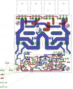
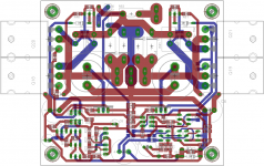
Layout
The board has undergone a redesign to reduce the length of high current traces by placing the bulk filter caps as close to the output transistor pins as close as possible. The pairs of output transistors are now horizontally opposed, whereas previously they were positioned along the top edge of the board. Subjectively, I believe that amplifiers with a large capacitance store close to the outputs sound better, and having the power supply on-board certainly simplifies wiring and chassis layout.
The LTP and current mirror transistors are oriented such that they can be thermally coupled (thanks Bigun).
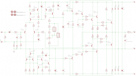
Circuit
LTP CCS has been cascoded to further reduce hum and I've settled on ~6mA for the LTP pair after analysing a number of similar designs that use this same family of input transistors.
The LTP cascode has been removed and higher voltage parts substituted for the LTP. I will experiment with cascodes in a future re-design; however, I believe this circuit is enough of a departure from the Mk I that I want to evaluate these changes in isolation.
I spent some time reading Groner on Self (http://www.sg-acoustics.ch/analogue_audio/power_amplifiers/pdf/audio_power_amp_design_comments.pdf) and a very interesting thread on this forum (http://www.diyaudio.com/forums/solid-state/133018-current-mirror-discussion.html). I've adopted an improved current mirror here. The emitter degen resistors have been redimensioned to drop approx. 660mV, which I feel is a reasonable compromise.
Its been a while since I updated this thread and in that time I've been very busy researching and refining this project.
Layout
The board has undergone a redesign to reduce the length of high current traces by placing the bulk filter caps as close to the output transistor pins as close as possible. The pairs of output transistors are now horizontally opposed, whereas previously they were positioned along the top edge of the board. Subjectively, I believe that amplifiers with a large capacitance store close to the outputs sound better, and having the power supply on-board certainly simplifies wiring and chassis layout.
The LTP and current mirror transistors are oriented such that they can be thermally coupled (thanks Bigun).
Circuit
LTP CCS has been cascoded to further reduce hum and I've settled on ~6mA for the LTP pair after analysing a number of similar designs that use this same family of input transistors.
The LTP cascode has been removed and higher voltage parts substituted for the LTP. I will experiment with cascodes in a future re-design; however, I believe this circuit is enough of a departure from the Mk I that I want to evaluate these changes in isolation.
I spent some time reading Groner on Self (http://www.sg-acoustics.ch/analogue_audio/power_amplifiers/pdf/audio_power_amp_design_comments.pdf) and a very interesting thread on this forum (http://www.diyaudio.com/forums/solid-state/133018-current-mirror-discussion.html). I've adopted an improved current mirror here. The emitter degen resistors have been redimensioned to drop approx. 660mV, which I feel is a reasonable compromise.
Attachments
- Status
- This old topic is closed. If you want to reopen this topic, contact a moderator using the "Report Post" button.
- Home
- Amplifiers
- Solid State
- My Blameless MkII