also looks rather pointless for those of us who don't have a fab - the circuits all use area ratio "current sense/replication" of well matching devices on a single substrate
I assume the Linear Audio article does not, unfortunately I left my copy somewhere at home. The first diagram on the patent looks like a replica sensing arrangement not totally unlike the start of some of the geometric mean biasers. If it wasn't for quasi-sat several of the xDSL drivers have little or no crossover to speak of even when deeply class A/B.
Last edited:
Great writeup . Note that Mr. Pass is left-handed.Here is a document that may be of interest. Denon used the optically controlled bias approach in some of their 90s integrateds (ie PMA-520). A schematic is available on hifiengine.com.
Dispersion is not the prerogative of optocouplers: all semiconductors have a good degree of variability, and this does not prevent the design of good electronics.I'm also not so sure of the optoisolator bias circuit feasibility requiring matching CTR - CTR relies on both LED emission and phototransistor hfe - not a formula for consistency, repeatability, stability
In this case, the variability of the CTR will only have benign effects; offset voltage in the Vf of the LEDs is potentially more troublesome, just as in any diff amp, but I have just made an informal test on a TIL193 quad opto, and all the 4 Vf's were comprised between 961mV and 962mV.
Maybe I've been lucky, but even if it is 10 times worse, it is still acceptable here.
Thanks Elvee for the clarification. I hope the explanation of how the circuit works is like my understanding below:The connections to a and b nodes are correct. c is just a reference point, unconnected to anything else for the time being.
I failed to discover where the optical part was hiding
- At idle, the dynamic resistance of the // connected optocoupler bjts [call it Rx] are also //connected with the resistor 1k5 across the emitter -base of the bias bjt. The idle bias voltage is [c-a = y]
- During signal conditions, the value of Rx decreases so as to move the bias bjt in the direction of cutoff.
- So, the collector-emitter voltage of the bias bjt increases to y'.
- This effectively means a Dynamic A bias; which may be devised to be limited in its range of action.
You may not be utterly wrong, but you are looking in the wrong direction.Thanks Elvee for the clarification. I hope the explanation of how the circuit works is like my understanding below:
- At idle, the dynamic resistance of the // connected optocoupler bjts [call it Rx] are also //connected with the resistor 1k5 across the emitter -base of the bias bjt. The idle bias voltage is [c-a = y]
- During signal conditions, the value of Rx decreases so as to move the bias bjt in the direction of cutoff.
- So, the collector-emitter voltage of the bias bjt increases to y'.
- This effectively means a Dynamic A bias; which may be devised to be limited in its range of action.
I thought the circuit was simple enough as to be self-explanatory, but that is to my eyes, and some explanation might be required after all.
There are hundreds of ways of looking at the way the circuit operates, but relying on equivalent resistances is probably one of the least helpful.
An optocoupler is essentially a CCS, with a dynamic resistance in the megohm range, and equating the static resistance to the dynamic resistance is not very helpful either.
If we neglect the opto couplers for the time being, the bias circuit is just a conventional one, except it is grossly underbiased: the OP devices have no chance of conducting simultaneously, and this results in heavy Xover distortion.
Any of the top or bottom active opto will conduct if the current in the collectors of the corresponding OP transistor is reduced too much: the bottom line being 1/2 of the current through R3 if the transistor in question is completely off.
This current is passed to the base spreader after a scaling by the CTR, and will impose an additional drop across R4 to keep the equilibrium of the base spreader.
This additional drop will also appear between the bases of the transistors controlled by the spreader.
Since there is NFB at work, the circuit will balance itself at a level determined by the constants of the circuit: mainly the values of R1 and R2, and the current through R3, and secondarily all the rest: the CTR's, the resistor values of the spreader, etc
One could compute the exact transfer function according to all the parameters, and perhaps shape it to achieve a geometric mean of the quiescent currents or similar.
I didn't go that far: at this stage, I am just interested in the mechanics of the circuit, and having the signs OK. Refinements may come at a later stage, at the moment the circuit is simply functional (which is not that bad after all)
Hi Elvee,
I confess to using optocouplers as zero crossing detectors in sort of linear regions years ago when I was designing (and patenting) mains based thyristor triggers for Clipsal now Schneider. Thus I understand your idea.
However the conceptual leap from zero crossing detector to a bias current clamp that only allows operation in Class AB mode at the point of zero crossing leaves me in awe. Congratulations and thank you for sharing.
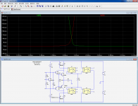
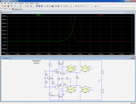
Anyway the idea interests me. So I modeled it, had a play and eventually converted my upgraded Leach 4.5 model (has 5 o/ps per side and all fast transistors used). Works delightfully more or less out of box.
What I found :-
>>Opto led current at operation needs to be designed, to suit the CTR and rail voltage
>>The existing bias multiplier needs to be left at optimum bias current for Vin = 0v at room temp (this is the max bias current that the clamp will allow)
>>The opto devices need a base emitter resistor (=100R) to minimise the charge storage time
>>Need to minimise the amplifier's output offset voltage to give the small signal operation some symmetry where it transitions from Class A to Class AB - otherwise the upper and lower zero crossings start to occur at different times leading to distortions.
>>With fast transistors the bias multiplier capacitor appears to be not needed although I have left it in circuit at 100n.
>>In spice at least I am seeing very low distortion from 1kHz to 50kHz
My next steps are to modify an actual upgraded Leach 5 per side, that I just happen to have on hand, to test the temperature behaviour and to see if it really does avoid thermal runaway. Parts orders are underway. I have very little test equipment and cannot measure distortion but static measurement of thermal effects is well within my scope.
If I may, I will keep you posted.
John
I confess to using optocouplers as zero crossing detectors in sort of linear regions years ago when I was designing (and patenting) mains based thyristor triggers for Clipsal now Schneider. Thus I understand your idea.
However the conceptual leap from zero crossing detector to a bias current clamp that only allows operation in Class AB mode at the point of zero crossing leaves me in awe. Congratulations and thank you for sharing.
Anyway the idea interests me. So I modeled it, had a play and eventually converted my upgraded Leach 4.5 model (has 5 o/ps per side and all fast transistors used). Works delightfully more or less out of box.
What I found :-
>>Opto led current at operation needs to be designed, to suit the CTR and rail voltage
>>The existing bias multiplier needs to be left at optimum bias current for Vin = 0v at room temp (this is the max bias current that the clamp will allow)
>>The opto devices need a base emitter resistor (=100R) to minimise the charge storage time
>>Need to minimise the amplifier's output offset voltage to give the small signal operation some symmetry where it transitions from Class A to Class AB - otherwise the upper and lower zero crossings start to occur at different times leading to distortions.
>>With fast transistors the bias multiplier capacitor appears to be not needed although I have left it in circuit at 100n.
>>In spice at least I am seeing very low distortion from 1kHz to 50kHz
My next steps are to modify an actual upgraded Leach 5 per side, that I just happen to have on hand, to test the temperature behaviour and to see if it really does avoid thermal runaway. Parts orders are underway. I have very little test equipment and cannot measure distortion but static measurement of thermal effects is well within my scope.
If I may, I will keep you posted.
John
Hi Johno,
Thanks for the feedback, you spare me another ugly prototype...
This surprises me:
Thanks for the feedback, you spare me another ugly prototype...
This surprises me:
Such a low value will shunt almost the totality of the photo-current generated in the BC junction directly to the emitter; I even doubt the transistor could turn on in these conditions, this means you must be using it as a photodiode. It seems radical to me, but the device will certainly be faster (with a CTR divided by the Hfe)>>The opto devices need a base emitter resistor (=100R) to minimise the charge storage time
Hi Elvee,
I confess to using optocouplers as zero crossing detectors in sort of linear regions years ago when I was designing (and patenting) mains based thyristor triggers for Clipsal now Schneider. Thus I understand your idea.
However the conceptual leap from zero crossing detector to a bias current clamp that only allows operation in Class AB mode at the point of zero crossing leaves me in awe. Congratulations and thank you for sharing.
Anyway the idea interests me. So I modeled it, had a play and eventually converted my upgraded Leach 4.5 model (has 5 o/ps per side and all fast transistors used). Works delightfully more or less out of box.
What I found :-
>>Opto led current at operation needs to be designed, to suit the CTR and rail voltage
>>The existing bias multiplier needs to be left at optimum bias current for Vin = 0v at room temp (this is the max bias current that the clamp will allow)
>>The opto devices need a base emitter resistor (=100R) to minimise the charge storage time
>>Need to minimise the amplifier's output offset voltage to give the small signal operation some symmetry where it transitions from Class A to Class AB - otherwise the upper and lower zero crossings start to occur at different times leading to distortions.
>>With fast transistors the bias multiplier capacitor appears to be not needed although I have left it in circuit at 100n.
>>In spice at least I am seeing very low distortion from 1kHz to 50kHz
My next steps are to modify an actual upgraded Leach 5 per side, that I just happen to have on hand, to test the temperature behaviour and to see if it really does avoid thermal runaway. Parts orders are underway. I have very little test equipment and cannot measure distortion but static measurement of thermal effects is well within my scope.
If I may, I will keep you posted.
John
Is there any thing to report on this?
- Status
- This old topic is closed. If you want to reopen this topic, contact a moderator using the "Report Post" button.
- Home
- Amplifiers
- Solid State
- Opto-controlled bias