Hi Patrick,
You can see the specs here.
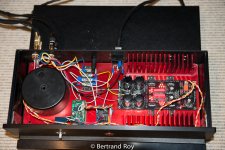
I'm not sure which are the smoothing caps. I am attaching a close up of the unit.
Blessings, Terry
The ones with the coils in between them and I already saw the capacitance thanks the pic
Last edited:
Jason,
On thing I'm curious about: On your schematic, the current for the feedback path is injected between the 100R and 2.2k resistor. On all the others, the injection node is between the cap to the common and the 100R. That would imply a difference in the impedance at that node. Not sure the significance but I looked around and couldn't fine any explanation for choosing one over the other.
Sheldon
Last edited:
Sheldon,
The current injection point doesn't seem to make much difference with respect to performace. It simmed with slightly (and I mean very marginal) less distortion so I thought I'd give it a try. There is slightly less DC voltage on the FB caps as well.
The choice is deliberate.
The current injection point doesn't seem to make much difference with respect to performace. It simmed with slightly (and I mean very marginal) less distortion so I thought I'd give it a try. There is slightly less DC voltage on the FB caps as well.
The choice is deliberate.
Sheldon,
The current injection point doesn't seem to make much difference with respect to performace. It simmed with slightly (and I mean very marginal) less distortion so I thought I'd give it a try. There is slightly less DC voltage on the FB caps as well.
The choice is deliberate.
Thanks,
I realized that after I posted. With a very high impedance source, the difference made by a 100R resister on either side would be proportionally insignificant.
Sheldon
All deliveries fulfilled
Thanks folks, every package reached its destination!
still4given - 2 - Delivered
ivanlukic - 2 - Delivered
quan - 2 - Delivered
triplej - 2 - Delivered
baswamin - 2 - Delivered
potepuh - 2 - Delivered
spind - 2 - Delivered
brianco - 2 - Delivered
Sheldon - 2 - Delivered
Sounds like a few of you have / may be starting builds, so if you have any comments, questions or suggestions feel free to throw it out there. Pics are good too .
.
Thanks folks, every package reached its destination!
still4given - 2 - Delivered
ivanlukic - 2 - Delivered
quan - 2 - Delivered
triplej - 2 - Delivered
baswamin - 2 - Delivered
potepuh - 2 - Delivered
spind - 2 - Delivered
brianco - 2 - Delivered
Sheldon - 2 - Delivered
Sounds like a few of you have / may be starting builds, so if you have any comments, questions or suggestions feel free to throw it out there. Pics are good too
.I'm forging ahead with some changes to the design and will post information when I have it. I'm open to suggestions to incorporate into the next iteration of the design should someone have input. I will add to post #1 to hopefully keep things organized and accessible over time.
For now I'm going to put up a ZIP of the Gerber and Excellon files of the current version, should someone choose to have additional ones made for themselves.
For now I'm going to put up a ZIP of the Gerber and Excellon files of the current version, should someone choose to have additional ones made for themselves.
Attachments
Don't no if it helps and save some labour. Links to member nikosokey's VSSA based on your PCB's Jason. He used fets/CSS and TLVH431, in fact looks near to LC's VSSA except layout/component choice, maybe PM nikosokey.I need to do some more reading........
http://www.diyaudio.com/forums/vend...lateral-mosfet-amplifier-184.html#post3556078
http://www.diyaudio.com/forums/vend...lateral-mosfet-amplifier-231.html#post3616830
http://www.diyaudio.com/forums/vend...lateral-mosfet-amplifier-232.html#post3618212
I need to do some more reading. I found some articles by Walt Jung pertaining to the subject of CCS types for audio. My only reservation about JFETs is what looks like continually dwindling availability and wide variances in parameters.
They do vary more than transistors, but it's really not an issue here, as each leg is individually adjusted anyway. Not hard to select parts if you wish, and the variance is typically much less within a lot than the specs. suggest. You still get, with fewer parts, higher impedance. I might add a gate resistor to the list of parts, but that's it.
Sheldon
Hi Guys, got boards up and running. On calibration vas current 15.4mA with DC offset at 2mV both channels. Is there any problem with running higher vas current?. I understand LC module recommended 12mV vas only. My psu is 45V+/-.
Quan
Thanks for the update Quan! Hope you can give us some review or insight into your build when you have had a chance to use them a bit. A pic would be
too.The VAS current, with proper heat sinking, could be as high as 20mA or higher if the device's parameter's support it. That isn't really needed and doesn't seem to improve performance. The ideal range seems to be anywhere from 12mA to 16mA, so an individual builder has some latitude and a precise value isn't really important. The adjusters should have enough range to get the VAS current down to 12mA if you so choose. Everyone's VAS devices were matched on a curve tracer to get overlapping traces in the recommended current range, which is why they were bagged separately.
Hello,
I'm rather new at DIY electronics. I have read through this thread and am very interested in your implementation of the VSSA. I have a few questions if I may:
1- There were a few suggestions about having part of the PSU on board. Will this be realized with a new implementation now that your first run is done?
2- Are there other improvements that you will be doing - you were mentioning reorienting the trim pots, etc.
The last comment/request I would make as I would really like to get some boards (at least 4) is purely aesthetics. I have built a DCB1 pre-amp but it was the "Black Edition" where the PCB was black and the components were red and black. I love that look. Would it be possible to make the PCBs a different colour through your supplier? Would it cost extra (I don't really care)? Just a thought as I think looks also count in DIY. Again, this is my personal opinion.
Thank you Jason for your contribution so that people far less experienced can benefit from great sounding amps.
Bye for now.
Bertrand
Hello,
I'm rather new at DIY electronics. I have read through this thread and am very interested in your implementation of the VSSA. I have a few questions if I may:
1- There were a few suggestions about having part of the PSU on board. Will this be realized with a new implementation now that your first run is done?
2- Are there other improvements that you will be doing - you were mentioning reorienting the trim pots, etc.
The last comment/request I would make as I would really like to get some boards (at least 4) is purely aesthetics. I have built a DCB1 pre-amp but it was the "Black Edition" where the PCB was black and the components were red and black. I love that look. Would it be possible to make the PCBs a different colour through your supplier? Would it cost extra (I don't really care)? Just a thought as I think looks also count in DIY. Again, this is my personal opinion.
Thank you Jason for your contribution so that people far less experienced can benefit from great sounding amps.
Bye for now.
Bertrand
Welcome Bertrand,
Let me answer your questions as best I can.
1) I'm planning on incorporating a low current CM (Capacitance Multiplier) to supply much cleaner power to the input pair and VAS transistors. I'm seeing that most of the CM PSU benefit can be realized more simply with the VSSA this way than by creating a high current dedicated CM PSU.
2) I'm looking at perhaps changing the CCS type but have not yet done all the research to render a decision on that yet. Also, some of my other comments related to making it more DIY-friendly by restricting the effective range of the trimmers and making their adjustment more logical with respect to their effect on the circuit. Also thinking about adding more options for connectors and expanding the range of component choices (mostly extra pads for different lead spacings and such).
As far as aesthetics go I'm sure the board house can do other colours for the boards and silk screen, and most certainly for a premium. Now, what colours and how much of a premium I do not know - I just went blase and got the usual green and white.
Other members have expressed interest so perhaps a new order of maybe another 20 pieces isn't out of the question to fill the current inquires plus spares. A new version isn't going to be next week, but it will appear eventually. I like to take my time and make sure things are as close to perfect as I'm able to manage.
Hope that helps.
Hi Jason,
Thank you very much for your prompt reply!
I really appreciate that you want things to be perfect before committing. It makes things easier for people like me.
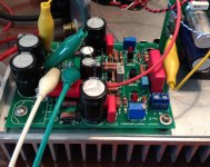
Quick question, I see that there are two To3 (the half round black things) that seem to be glued together on your board. Why is that when the others are spaced apart?
I may just have divulged how much of a newb I am...
Thanks.
Bertrand
Thank you very much for your prompt reply!
I really appreciate that you want things to be perfect before committing. It makes things easier for people like me.
Quick question, I see that there are two To3 (the half round black things) that seem to be glued together on your board. Why is that when the others are spaced apart?
I may just have divulged how much of a newb I am...
Thanks.
Bertrand
Quick question, I see that there are two To3 (the half round black things) that seem to be glued together on your board. Why is that when the others are spaced apart?
I may just have divulged how much of a newb I am...
Bertrand
There are two transistors glued together. The small black package is actually a TO-92, a TO-3 is a large metal can bolted down through holes in its flange.
The ones that are glued together are the input pair. In this design there is some advantage to thermally coupling these devices to keep the DC offset at the output low. Some use thermal paste and heat shrink on these while others just glue them. I use the tiniest drop of an instant adhesive (Krazy Glue™ or similar ethyl cyanoacrylate product) to make my two devices one.
The others are for the CCSs and we don't want these coupled together to help keep the current flowing in the CCSs the same. A 2Q CCS is thermally sensitive and the transistor in control of the current dissipates much less power than the transistor that feeds the current to the rest of the circuit. We don't want one affecting the other, so we keep them apart.
No worries about being new to the hobby. I will always have the time for someone willing to put in some effort to learn and grow in knowledge and experience. I have requested some information about board options to see how the price is affected and will post back when I know something. Right now the Chinese New Year is on, so I can't get any answers until celebrations are finished.
Hi Jason,
Thank you so much for taking the time to explain that! My lightbulb dimmer is now a notch up!
Thank you also for taking the time to check into a new order and colours. I put in a picture of my DCB1. I also anodized the aluminium. In my opinion, red and black look great. I'm having an Optix cover made tonight at a friend's. He has a home laser CNC...
Thanks again.
Bertrand
Attachments
Got the boards assembled and one mounted and adjusted. I substituted a standard red LED for Q3,6 (MV50640). Solders right into the PCB, across the emitter/collector position for Q3,4. For the LED, a standard red is best, as it has the lowest dynamic resistance for LEDs, of about 4R. The LED drops about 1.8v, so VR1,3 should be 1k. I used 3.6k for R11,12 to get about 9mA current in the LEDs for a 36V supply. This current level gets the LED well into its linear impedance range.
Took me a bit to get all the bias levels lined up and offset within the low single digit mV range. Offset wanders a bit within that range during warm-up, but bias is quite stable.
Nice work Jason.
Took me a bit to get all the bias levels lined up and offset within the low single digit mV range. Offset wanders a bit within that range during warm-up, but bias is quite stable.
Nice work Jason.
Attachments
- Status
- This old topic is closed. If you want to reopen this topic, contact a moderator using the "Report Post" button.
- Home
- Amplifiers
- Solid State
- VSSA Through-Hole Version by Jason