going to play with a 200ohm 1/2W potentiometer. I sourced two pieces on EBAY Dale T18 200ohm 10% 25 turns for $3 delivered. I can set for 150ohms on the bench, value of the resistor being used currently for bias adjust, and connect to the sockets on the Input card. Measure bias voltage across bias resistor and tweak pot to higher resistance to lower the bias voltage. If anything else this might give me some idea how much resistance change might be required. If I get this set up will publish results.
Be aware potentiometers are good for adjusting bias, but bad for running the amp over the years. If you only hook up the wiper where the resistor should have gone, then if the wiper loses contact, bias current (usually) goes very high. If you short the wiper to one end of the pot, and the wiper loses contact, then the bias goes high but to a lower value. High bias current of course, causes excess heating of the output transistors. Wipers lose contact based on the oxidation of copper or tin, which is fairly inevitable. Only gold, palladium, rhodium etc contacts don't oxidize, and few potentiometers have these materials used as contacts.
The ideal solution is to find out what value is required, then install resistors at that value instead of a potentiometer. Very sophisticated bias control circuits put a temperature sensor on the heatsink of the output transistors then reduce the bias current based on hot transistors. This requires some sort of negative temperature coefficient resistor usually, of which one type is the silicon diode.
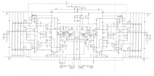
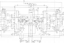
I've downloaded the DC300a schematic diagram from eserviceinfo.com, but am unable to spot the bias control network. I suppose somewhere the manual tells you where to change the resistor to change it. I see a summing resistor on the emitter resistors which goes to something like a VI limiter, but don't fully understand it. I don't see any sort of temperature sensing arrangement.
Last edited:
Channel 2 Q208(bias servo transistor) is on the heat sink. Agreed R220 has "SEL" next to it. I have not looked that far upstream. Have not taken any measurements on the Input card since replacing channel 1 pre driver transistors and repairing the collector feed circuit trace on the positive pre driver. Remember the neg pre driver failed double diode test (open) and the pos pre driver with the opened collector circuit tested double diode test okay. Both pre drivers were replaced with new transistors.
Resistor R230/R130 (emitter resistors neg pre drivers on input card) and R232/R132(emitter resistors pos driver on output board).
Tonight I can measure voltage across R230/R130(emitter resistors neg pre drivers on input card).
R232/R132(emitter resistors pos driver on output board) are described in the Crown manual as "bias level" measurement. The manual shows a 310-340mV measurement as good. I have measure R132(emitter resistor pos driver on channel 1 output board) and measured 410mV, exceeding the 310-340mV allowable. In the manual it says that increasing the value of R129 (ch1) or R229 (ch 2) will reduce the bias voltage measurement. These resistors are in sockets to allow hand selection. R129 (ch1) measured 150 ohms. This is the resistor I could use the 200 ohm pot to determine how much of an ohm change will be required to reduce the bias measurement.
Will reducing this "bias level" on channel 1 possibly reduce the current .7V DC offset?
The early part of your manual says an acceptable idle DC output voltage is .01 v.
When transistors fail, they allow high voltage to leak out the base lead into devices ahead of them that might not be rated for the voltage or wattage, thus blowing them up.
I wouldn't try to solve a .7 v output offset with bias adjustment resistors without thorough study of the other parts. Some of them might be blown up, ie open or shorted.
To start with, you may have a real leaky output transistor, that is causing the feedback circuit to bias the output the other way. That is why I want you to check the voltage on the output resistors on the bad side individually, each of them, all eight, not at the summing resistor place, R232 R230.
then after you have eliminated that as a problem, go back to IC1 and make sure the output is resting at 0 v. It is possible the adjust ment pot there will affect this, or it is possible something is blown between IC1 and the predriver. I had lots of little glass diodes blown, a few resistors blown, a couple of film and ceramic caps blown open. It is not just resistors that blow up.
Last edited:
wish I had checked them before I soldered them all in place. Newbie just assumed new transistors were a good starting point. Knowing that I have to de-solder them doesn't change what you are suggesting? I am going to do this your way since you have supported me in this since the beginning. Now as usual I need more detail in how you set up for the Vce test. You use one voltage supply. What voltage level do you use? Are those resistors selected to allow current to flow from the collector to resistor. ground the emitter to the neg side of the power supply. Bear with me..... thanks
Last edited:
Bias does not affect DC offset.
There is a DC offset control around the opamp.
The correct bias is 340mV on the bases of the outputs, this is zero bias in the outputs, and about 60mA through the drivers (TO-3 devices).
For reliability:
Replace the 10V zener diodes for the opamp.
Replace the series 10µF/160V in the voltage doubler circuit.
Replace the CCS transistor (fed from the doubler circuit) on the positive rail on both channels.
Indianajo, measured R130 at .61V and R230 at .65V.
djk, I should use the dc balance pots to remove the .7V on channel 1?
Voltage across the output emitter resistors are 0V. The suggested bias setting measurement is taken across the driver emitter resistor and should be between 0.31 and 0.34mV as shown on the schematic?
I should increase value of hand select resistor to lower bias measurement of Channel 1 from 0.41V to the required 0.31 to 0.34V. I will renew the voltage doubler circuit. Suggested replacement diodes, capacitor, and transistors. I did purchase the one 10V zener diode.
Last edited:
As I said, I could care less what R130 and R230 read. I did not ask you to unsolder anything. I want you to measure the voltage across R115, R116, R117, R118, R133, R13blob, R13blob, and R137. Then divide by .33 ohms to see what the current is in each. Are they balenced?
The matching Vce test could have been before you installed them, but now you just need to see if there is an imbalance problem. These resistor numbers are for one channel, they are different on the other. I want you to measure the emitter resistor voltage on the channel that has the offset.
I measure things before I go unsoldering the bases to see if I am going to replace them. The 10 uf cap dke mentions should go just based on the calender, as measurements on old wet caps are not valid due to the deterioration of rubber seals after twenty years.
These people on here throw terms around like CCS that I don't know what they are talking about. Q10blob might be a constant current source, since it has a resistor R131 between base and emitter. It is certaainly in a place where it could be blown up by bad output transistors. So is the resistor, which should be measured.
I found zener diodes that measured about 700 ohms forward (0.7 v on my meter) and infinity backwards out of circuit were dropping the proper voltage forwards with the power on. You can certainly measure D4 in circuit to see if it is dropping 10 v. Every other diode and resistor can be measured with the power on, so see if you get a plausible reading. Diodes d102, d103, 104, 105 are just as likely as anything to be blown up as anything. The nearer to the output transistor, the more likely stuff is to be blown up.
Does the statement "using DC balance pots DC off set for channel 1 and channel 2 is 0 v" mean you have solved your 0.7v on speaker output problem?Which channel was the one with the problem? Why are you messing with the other one? What is the output of the IC1 on the bad channel?
"Then divide by .33 ohms to see what the current is in each. "
The Crown DC300A runs class AB+B, there is no bias in the output stage.
340mV on the bases of the outputs puts the drivers in class AB with about 60mA of current (340mV across 5.6Ω).
It's a good idea to replace both the zener diodes that power the opamp, the parts I mentioned are all common fail items, do you want to open it up again in a month or two?
- Status
- This old topic is closed. If you want to reopen this topic, contact a moderator using the "Report Post" button.
- Home
- Amplifiers
- Solid State
- Crown DC300A Repair/Restore


