Jeff , I want your opinion (as a "men of action" type).
On -
The fast-ons .... I made a special solder mask to really make them
hardy with strain relief.
My take on JK's artwork - I had to redraw all to sprint 5. Does
sprint 5 have any issues/conflicts with the board houses ?
My decoupling - I ditched the 10 small caps at the output collectors
and have a much bigger set of caps right in the middle of the rails , decoupling
should electrically be the same ... less soldering.
My BJT/FET option setup. Bridge the "B" SMD pads. I could not think
of a better way to make for this changover.
Any other wants/suggestions , the board matches the original + 25mm
most holes line up perfect (with JK's V1.3).
I'm labeling now.
OS
A Keystone 7797 might be a nice replacement for the Fastons at the power inlets. The Faston will still go into the same holes but it gives you the option for a solid screw down connection. 7797 Keystone Electronics | Mouser
The board houses can work with just about anything for Gerber files. Sprint 5 is definitely okay.
I keep looking at your cap but didn't want to say anything. Those cap traces are going to be very high current areas with the caps charging and discharging though the same path with every voltage fluctuation. I think it would be better to have a large reservoir right at the inlet and smaller decoupling caps right at the output devices.
Bridging smt pads works great for selecting options. I've been thinking of doing the same an my DAC design instead of jumpers.
It looks like the heat dispersion will be much better with this one. Q104 will be right up in the middle of all the heat so it will likely react sooner as well.
One minor bug I can see is the base resistor leads on the two lower output devices. Can they get close to the collector leads on the transistor below if the guy assembling isn't watching closely? Could the resistor pad be centered over the base lead below?
Esperado likely won't like you takeoff point for the NFB. Can it go right at the inductor coil? It won't really be seeing what the speaker is getting if it's coming from the between the emitter resistors.
Don't worry sync. My kids all lost my parts , blew up projects with water ...
even 3 of 4 (yes , I have 4!) burned themselves with soldering irons when young.
But , they knew hot/burn at 5 , and never touched stoves or fires after that.
At 8+ years , it was worth the trouble - they are quite "carefree" (even
help out) .
OS
even 3 of 4 (yes , I have 4!) burned themselves with soldering irons when young.
But , they knew hot/burn at 5 , and never touched stoves or fires after that.
At 8+ years , it was worth the trouble - they are quite "carefree" (even
help out)
.OS
A Keystone 7797 might be a nice replacement for the Fastons at the power inlets. The Faston will still go into the same holes but it gives you the option for a solid screw down connection. 7797 Keystone Electronics | Mouser
The board houses can work with just about anything for Gerber files. Sprint 5 is definitely okay.
1. I keep looking at your cap but didn't want to say anything. Those cap traces are going to be very high current areas with the caps charging and discharging though the same path with every voltage fluctuation. I think it would be better to have a large reservoir right at the inlet and smaller decoupling caps right at the output devices.
Bridging smt pads works great for selecting options. I've been thinking of doing the same an my DAC design instead of jumpers.
It looks like the heat dispersion will be much better with this one. Q104 will be right up in the middle of all the heat so it will likely react sooner as well.
2-One minor bug I can see is the base resistor leads on the two lower output devices. Can they get close to the collector leads on the transistor below if the guy assembling isn't watching closely? Could the resistor pad be centered over the base lead below?
3-Esperado likely won't like you takeoff point for the NFB. Can it go right at the inductor coil? It won't really be seeing what the speaker is getting if it's coming from the between the emitter resistors.
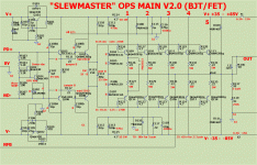
Excellent .... what I wanted.
1 - those are double sided 8.5A Imax traces. What ripple would exceed
17A ? Main traces are double 16A , there should be almost no L or R ?
I looked at the Pass IRFP OPS , just fat tracks and 2 big caps.
Another mm maybe ? (20+A Imax).
Keentoken mentioned that the L/C/L /C/L/C .... of a trace/capacitor/trace
can also lead to ringing with heavy load (and a smaller C <1uf).
A consensus of big high-end OPS's , I see fat traces , big caps and strategically placed .1uf 's at distance from the main decoupling.
Also , non-inductive main output Re's are quite standard.
2 - elaborate (with what you mean circled ).
3 - I agree , I'm working on it.
PS - thanks for the connector link ..... I'll see if I have to fine tune the
artwork to make these usable.
OS
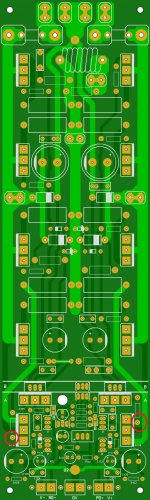
The two red circles at the bottom Is where I am talking about with the base resistors.
But they are not touching .... oh , if the through hole lead is long (I got it).
and the last post..
I agree , If I swap the 3A diodes with the cap position .... I'll be right at
the rails.
Thanks.
Edit - i don't understand ? "reversing down the same path" , each rail cap just "sees" half wave
ripple ?
Last edited:
What are the Fastons right at the diodes in the middle of the rails for?
One other good addition would be a Bias connector for the protection boards. We've been using these with the keyed side to negative. MOLEX 39-28-1023 Mini-Fit Jr. Header, 2 Row, Vertical, w/o Snap-in Plastic Peg PCB Lock, 2 Way, w/o Drain Holes
One other good addition would be a Bias connector for the protection boards. We've been using these with the keyed side to negative. MOLEX 39-28-1023 Mini-Fit Jr. Header, 2 Row, Vertical, w/o Snap-in Plastic Peg PCB Lock, 2 Way, w/o Drain Holes
I was near to suicide ;-)E3 - I agree , I'm working on it.
Edit - i don't understand ? "reversing down the same path" , each rail cap just "sees" half wave
ripple ?
The current comes in through that trace when the rail voltage is high. When current is consumed by the output devices it needs to go back out the path it just came in on. If it has another path leading to the output devices it will flow that way instead. Current will flow in one trace and out the other in one direction instead of reversing with every cycle.
Randy Slone explained it better. I'll see if I can find his explanation and pass it on. I've seen AndrewT point this same thing out in supply cap wiring as well.
Last edited:
What are the Fastons right at the diodes in the middle of the rails for?
One other good addition would be a Bias connector for the protection boards. We've been using these with the keyed side to negative. MOLEX 39-28-1023 Mini-Fit Jr. Header, 2 Row, Vertical, w/o Snap-in Plastic Peg PCB Lock, 2 Way, w/o Drain Holes
"Arc welder mode"
OS
On the contrary, to the heartI've got your back.
Perfect!Jeff , I want your opinion (as a "men of action" type)
On -
The fast-ons .... I made a special solder mask to really make them
hardy with strain relief.
My take on JK's artwork - I had to redraw all to sprint 5. Does
sprint 5 have any issues/conflicts with the board houses ?
My decoupling - I ditched the 10 small caps at the output collectors
and have a much bigger set of caps right in the middle of the rails , decoupling
should electrically be the same ... less soldering.
My BJT/FET option setup. Bridge the "B" SMD pads. I could not think
of a better way to make for this changover.
Any other wants/suggestions , the board matches the original + 25mm
most holes line up perfect (with JK's V1.3).
I'm labeling now.
OS
Just keep it as DIY friendly as possible.
Perfect!
Just keep it as DIY friendly as possible.
Yes , and ask your peers for evaluation/critic.
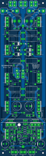
I even like it better with Jwilhelms advice added. Looked at more OPS's
and read some Slone.
Now it looks "mean".
Has those Keystone "arc welder" hookups - and the molex for protection. NFB is right. A perfect star (G1).
All is below , I think it's 100%.
OS
Attachments
Strange. Well, I had hoped it would work for you. My apologies that it did not.
It might of tried updating or some other BS. It actually caused the first single
program crash in my new PC's 2 year history (Win7-64) ???
It worked long enough for me to
ascertain that it's not worth upgrading.
5 is faster , smaller - 6's few paltry improvements .... I would not pay $$$
for them. Not your fault.
Software is a "racket" ....
OS
Just as a counterpoint, I've been using Sprint Layout 5 and now 6 for the last few years. I've logged many hours with it and have never had a problem. Most recently I have been using it on the Windows 10 beta. Of the 3 PCB CAD packages that I have used over the years Sprint Layout is the easiest to use. My only grumble is that it doesn't have a schematic layout tool to keep me from making the wrong connections when laying out the PCB. Argh ...
- Home
- Amplifiers
- Solid State
- Slewmaster - CFA vs. VFA "Rumble"