Hi all!
Does anyone has made amplifiers under this schematic?
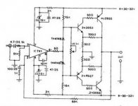
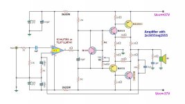
Is this is a good schematic (circuit) and should make some changes for the power supply for the Ucc=+/-40V?
Is this Schematic-N is better?")
Thank you for your cooperation!
Does anyone has made amplifiers under this schematic?
Is this is a good schematic (circuit) and should make some changes for the power supply for the Ucc=+/-40V?
Is this Schematic-N is better?
Thank you for your cooperation!
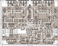
Attachments
Last edited:
cant vouch for the rest of the circuit, but I can say that with the supply to the opamp regulated as shown, its not going to explode at all, and if the zener is suitably rated the 2k resistor is fine. Ohms law if you want proof, but 25 volts across a 2k resistor is going to generate around 1/3 of a watt of heat. Smoke is an unlikely result.
According to the datasheet the 741 is internally compensated for unity-gain and pin 8 is not connected. So the 10pF capacitor is useless.
Its slew-rate is also on the low side (0,5 - 0,7V/µs). This gives an over-all slew-rate of max. 5V/µs. A NE5534 (with those 10pF or more) will give better results.
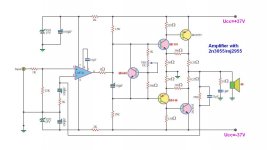
The second schematic should have better thermal stability but the component values of the bias-spreader are not correct (BD689 is a Darlington, VR1 should be placed in the B-E branch).
Its slew-rate is also on the low side (0,5 - 0,7V/µs). This gives an over-all slew-rate of max. 5V/µs. A NE5534 (with those 10pF or more) will give better results.
The second schematic should have better thermal stability but the component values of the bias-spreader are not correct (BD689 is a Darlington, VR1 should be placed in the B-E branch).
The 2nd schematic looks more promising, but the 3055 is not able to handle the +/-40V supply.
Generally it's very simple, and well known topology.
Sajti
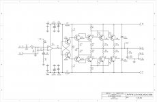
To replace 2n3055/mj2955 with MJ15003/MJ15004?
Is it possible BD679 can be replaced with BD139 and IC LM741 be replaced with a TL071?According to the datasheet the 741 is internally compensated for unity-gain and pin 8 is not connected. So the 10pF capacitor is useless.
Its slew-rate is also on the low side (0,5 - 0,7V/µs). This gives an over-all slew-rate of max. 5V/µs. A NE5534 (with those 10pF or more) will give better results.
The second schematic should have better thermal stability but the component values of the bias-spreader are not correct (BD689 is a Darlington, VR1 should be placed in the B-E branch).
This schematic-NEW gave it right?
thanks!
Last edited:
Since the output stage is a feedback pair (common emitter) then the op amp is not responsible for the voltage gain. A lower voltage source for the op amp is required and will not affect the limit of the output voltage swing. Sure the resistor's current drops out the voltage but at the instant of power up, destructive voltage could possibly occur across the op amp. It is just good practice and good for reliability in electronics that devices, especially BJTs are not subject to Vceo breakdown voltages as it reduces the life expectancy significantly.
This schematic-NEW gave it right?
thanks!
I think, that it's ok for starting project for a beginner diyer.
Sajti
This schematic-NEW gave it right?
thanks!
One notice only: Change VR1 to 2.2kohm.
Sajti
Safety first: add a resistor to VR1.Change VR1 to 2.2kohm.
Safety first: add a resistor to VR1.
Maybe yes, but it's not necessary, if he set the bias carefully.
Sajti
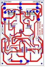
Attachments

Here is a link to the one that I made a while back,
http://www.diyaudio.com/forums/chip...own-supply-what-could-happen.html#post3695968
It worked good.
I will be using a ADA4700-1 high voltage opamp on the next version in order to get more voltage swing out of it.
http://www.analog.com/static/imported-files/data_sheets/ADA4700-1.pdf
jer
http://www.diyaudio.com/forums/chip...own-supply-what-could-happen.html#post3695968
It worked good.
I will be using a ADA4700-1 high voltage opamp on the next version in order to get more voltage swing out of it.
http://www.analog.com/static/imported-files/data_sheets/ADA4700-1.pdf
jer
Last edited:
- Status
- This old topic is closed. If you want to reopen this topic, contact a moderator using the "Report Post" button.
- Home
- Amplifiers
- Solid State
- Audio amplifier with uA741 and 2N3055/MJ2955