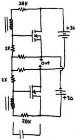
Now the secondaries of the transformer have been moved so that the MOSFETs work as a source-follower. I'm a bit uncomfortable running the transformer secondary through the bias resistor, so an AC coupling cap can be added on top and bottom (example bottom capacitor shown).
The bias is uncontrolled; the 28k and 2k resistors give about +2V on the base of the FETs. The bias current (~1mA) flows through the transformer secondary.
I didn’t draw the grid stoppers, ect … so don’t start being picky.
Notice that voltage variations in the power supplies will cause DC offset.
My next installment will study joining the power supply, to a single bipolar supply. Once that’s done, all that’s left is establishing DC bias control, and maybe a bit of local feedback.
Attachments
Here is other links of CSPP , If you known Japanese:
http://www.ne.jp/asahi/evo/amp/CSPP/2SJ18.htm
http://www.hinocatv.ne.jp/~s_suzuki/Uni_CSPP/J114/J114CSPP.htm
http://www.ne.jp/asahi/evo/amp/CSPP/2SJ18.htm
http://www.hinocatv.ne.jp/~s_suzuki/Uni_CSPP/J114/J114CSPP.htm
Subwo1, like this?
http://www.diyaudio.com/forums/showthread.php?postid=35226#post35226
http://www.diyaudio.com/forums/showthread.php?postid=35226#post35226
Kashmire has my disease. Buahahaha!!
") Good cct for mentally chewing over too. http://www.diyaudio.com/forums/showthread.php?s=&threadid=10658&highlight=
Good cct for mentally chewing over too. http://www.diyaudio.com/forums/showthread.php?s=&threadid=10658&highlight=
This way works really well!Kashmire said:My next installment will study joining the power supply, to a single bipolar supply.
Good cct for mentally chewing over too. http://www.diyaudio.com/forums/showthread.php?s=&threadid=10658&highlight=Circlotron, yes, that does seem to be the type of thing I was thinking of. Just out of curiosity, would you have a diagram?Subwo1, like this?
http://www.diyaudio.com/forums/show...35226#post35226
OK – Time to join the power supplies. Sorry Circ’.
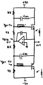
Going back to the first schematic, look at just the biasing scheme. If a resistor ladder is used, +4V can be applied to the MOSFET gate-to-source on both N-channels (see schematic below). An op-amp servo loop can control the middle of the voltage divider, in order to maintain zero DC offset at the output.
The op-amp strives to force the inverting input (-) to match the noninverting input (+). Since the noninverting input is connected to ground, the op-amp modulates the bias voltage on the resistor divider to keep the output at ground potential. Since you don’t want the op-amp to damp the AC output signal, a capacitor is used to set the time constant of the servo loop.
If the power supply voltages drift, the bias current will drift. It may be useful to have an absolute voltage reference for the voltage divider. The second circuit uses a zener diode for reference. This setup will allow for 8 volts of drift in the power supply, while keeping +4V gate-to-source on the MOSFETs.
The next message will be applying the signal to the circuit.
Attachments
Now to apply the signal. There are multiple options. My first schematic I posted has one method.
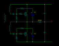
The circuit below applies the signal gate-to-drain. The signal appears over the secondary of the interstage transformer at the gate. The circuit is completed by the AC coupling capacitor Cac to the drain.
The AC coupling capacitor is the ultimate in local feedback for the MOSFET, functioning somewhat like connecting a pentode as a triode (vacuum tubes). The local feedback eats up all of the transistor’s available gain, resulting in the system operating in unity-gain. This is called source-follower mode. Therefore, the driver stage will have to provide all of the voltage gain. In this case, somewhere around 15 V/V would work well. I didn’t include a schematic of the driver stage, but I would start with a single-ended triode or triode-connected pentode.
I didn’t draw the gate stopper resistors. I assume 100 Ohms would work. I’d also include some 20k resistors to load the transformer secondaries.
A zener diode (see previous) could provide an absolute reference to the bias resistor divider. Switchable bias resistors could have two settings, “ice cube” and “pottery kiln”, depending on if you want 1A or 2A of bias current. Since this amp could work as class AB, as little as a few mA of bias current is actually required for operation. It would be a very cool amp, but wouldn’t sound that good. This functionality would be very useful, because the amp could run cool for everyday operations (television) and hot for critical listening. This is the one feature that the Zen amp designs don’t have.
Using source resistors (0.25 Ohms) would add a bit of stability and provide some local feedback. I added these to the schematic. In addition, they provide a good place to measure bias current. Another DC servo and voltage reference could be implemented for precise bias current control. That’s overkill for me.
I expect to model this circuit over the next few days.
Attachments

Kashmire said:
A zener diode (see previous) could provide an absolute reference to the bias resistor divider. Switchable bias resistors could have two settings, “ice cube” and “pottery kiln”, depending on if you want 1A or 2A of bias current. Since this amp could work as class AB, as little as a few mA of bias current is actually required for operation. It would be a very cool amp, but wouldn’t sound that good. This functionality would be very useful, because the amp could run cool for everyday operations (television) and hot for critical listening. This is the one feature that the Zen amp designs don’t have.
And then again...SOZ is actually sporting the option to have a moderate dissipation for everyday use and cruel dissipation for ...hmm...NICE use
All you gotta do is to build it with 2 sets of secondaries on the trafo, if im not mistaken it will run as low as 8 volts, thats not too bad. Then you can switch in between those two settings.
Magura
Hi All,
Last weekend I completed a bread board version of the second schematic of this page from the TubeCad website:
http://www.tubecad.com/index_files/page0021.htm
The input transformer I got from Sowter and is a 1CT:2+2. The Mosfet are a pair of semi matched BUZ11 and for the centertapped choke I use 2 gapped 125mH chokes.
On my way to work today I was thinking about the input circuitry of this amp and in particular about the AC currents that flow through this part of the amp when music is playing. It appears to me that this current is flowing through the power supply.
Would it be a wothwhile modification to decouple the input circuit with a good quality capacitor running from the input tranformer CT to the positive supply rail?
Or am I completely wrong here?
drive???
Kashmire,
I was looking at the circuit in post #1. By taking the output pos. half from source of one transistor and neg. half from drain of other transistor, the top one is a voltage follower and the bottom is a common source. The drive voltage for the top must be much larger than the bottom because the common source has a voltage gain (Av).
Try using complementary N-channel and P-channel devices either in common source or source follower, you might get a more symetrical sine wave signal.
or in the topology that you have there, maybe using class A for the top bias and the bottom transistor as a current source, output at 0 VDC.
I have start a new thread regarded this:
"Only N-Channel MOSFETs (NMOS); better Audio from non complements by Audio Power?" please go to
http://www.diyaudio.com/forums/showthread.php?s=&threadid=148646
"Only N-Channel MOSFETs (NMOS); better Audio from non complements by Audio Power?" please go to
http://www.diyaudio.com/forums/showthread.php?s=&threadid=148646
- Status
- This old topic is closed. If you want to reopen this topic, contact a moderator using the "Report Post" button.
- Home
- Amplifiers
- Solid State
- Push-Pull using only N-Channel MOSFETs