Hello people,
I am planning an analog amp module for active speaker. My idea is to develop an amp running in class-B.
Why class B?
Because thus the power loss remains low in two or three modules.
Why analogy?
Less high-frequency problems and is easier to implement in DIY. I also want to run the amp in the inverting mode. An inverting amplifier has a virtual ground at the input. Thus, there is less mass problems. Of the lower common-mode distortion aside.
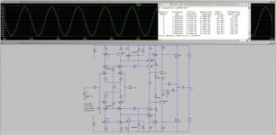
Here is a first idea I want to share with you. Nothing really new, but the circuit operation has low distortion in B-class (very hight open loop gain). By the way, class-AB is also possible. The bias can be set with R23.
The circuit is a ordinary symmetrically VFB-amplifier. It is only a little bit different at the current amplification. This is a transconductance amp, so another advantage is the output rail to rail.
I have tested many different compensations but really stable is it not.
If anyone knows how to do it better, show it please. Currently you definitely cannot drive capacities without coil/resistance at the output.
I am planning an analog amp module for active speaker. My idea is to develop an amp running in class-B.
Why class B?
Because thus the power loss remains low in two or three modules.
Why analogy?
Less high-frequency problems and is easier to implement in DIY. I also want to run the amp in the inverting mode. An inverting amplifier has a virtual ground at the input. Thus, there is less mass problems. Of the lower common-mode distortion aside.
Here is a first idea I want to share with you. Nothing really new, but the circuit operation has low distortion in B-class (very hight open loop gain). By the way, class-AB is also possible. The bias can be set with R23.
The circuit is a ordinary symmetrically VFB-amplifier. It is only a little bit different at the current amplification. This is a transconductance amp, so another advantage is the output rail to rail.
I have tested many different compensations but really stable is it not.
If anyone knows how to do it better, show it please. Currently you definitely cannot drive capacities without coil/resistance at the output.
Attachments
Hi Andrew,
good question. At the the emitters of the complementary LTP is a voltage about 600mV over/under ground. The positiv LTP -600mV and the negativ LTP 600mV. So there is a voltage of 1,2V. Now the direction clear. R23 loaded the complementary LTP and 'robs' the current. High current in R23, low bias of the whole amp.
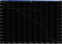
At first I thought that is a good idea, but after some simulations I recognize that with the bias setting also the frequency stability is greatly influenced.
Now I'll make it up conventionally") I also found a better compensation and now I think it is worth to developing a board.
I also found a better compensation and now I think it is worth to developing a board.
good question. At the the emitters of the complementary LTP is a voltage about 600mV over/under ground. The positiv LTP -600mV and the negativ LTP 600mV. So there is a voltage of 1,2V. Now the direction clear. R23 loaded the complementary LTP and 'robs' the current. High current in R23, low bias of the whole amp.
At first I thought that is a good idea, but after some simulations I recognize that with the bias setting also the frequency stability is greatly influenced.
Now I'll make it up conventionally
I also found a better compensation and now I think it is worth to developing a board.Attachments
repeat of the other two questions?what bias is the input set to?
what bias is the VAS set to?
You forgot to fit some elementary resistors. In such a topology will be REQUIRED to be some resistors 0.22Ohm - 5W attached to the source terminal of MOSFET's.
On the other hand, you have basically built the above schematic ? As you draw schematic, most likely oscillates in dynamic operation mode.
On the other hand, you have basically built the above schematic ? As you draw schematic, most likely oscillates in dynamic operation mode.
@Andrew
Maybe I expressed myself a bit clumsy, but both currents depend on the setting of R23.
Not so in the current Schematic...
The current source in the input has 3.3mA and the VAS has 2.4mA. Easy to finf out with the acs file
@ Thanks padamiecki,
you are right and I am looking for better comp. It looking much better when there is a big capacitor in the input and when the not inverting input is direct on ground. But then LTspice calculate and calculate and .... (some undefined conditions).
@ Hi donpetru,
if you drive only one pair it is not compelling to use source resistors. I plan instead of the resistor a fuse. And the thermal stability is determined by the emitter resistance of Q13/14.
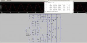
Attachments
Hi
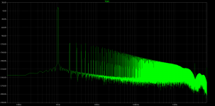
when r23 goes to 10 ohm, the idle at output irfs rise to ~150mA
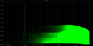
look at fft, it is GREAT
but still this oscillation
thd:
N-Period=1
Fourier components of V(vout)
DC component:-0.0039367
Harmonic Frequency Fourier Normalized Phase Normalized
Number [Hz] Component Component [degree] Phase [deg]
1 1.000e+03 6.600e+00 1.000e+00 179.99° 0.00°
2 2.000e+03 2.443e-06 3.701e-07 -7.93° -187.92°
3 3.000e+03 2.363e-06 3.581e-07 -93.36° -273.35°
4 4.000e+03 1.316e-06 1.993e-07 -2.84° -182.83°
5 5.000e+03 2.185e-06 3.310e-07 -92.21° -272.20°
6 6.000e+03 4.074e-08 6.173e-09 82.09° -97.90°
7 7.000e+03 5.329e-07 8.074e-08 -92.81° -272.80°
8 8.000e+03 7.618e-07 1.154e-07 176.64° -3.35°
9 9.000e+03 3.520e-07 5.333e-08 88.30° -91.69°
Total Harmonic Distortion: 0.000066%
when r23 goes to 10 ohm, the idle at output irfs rise to ~150mA
look at fft, it is GREAT
but still this oscillation
thd:
N-Period=1
Fourier components of V(vout)
DC component:-0.0039367
Harmonic Frequency Fourier Normalized Phase Normalized
Number [Hz] Component Component [degree] Phase [deg]
1 1.000e+03 6.600e+00 1.000e+00 179.99° 0.00°
2 2.000e+03 2.443e-06 3.701e-07 -7.93° -187.92°
3 3.000e+03 2.363e-06 3.581e-07 -93.36° -273.35°
4 4.000e+03 1.316e-06 1.993e-07 -2.84° -182.83°
5 5.000e+03 2.185e-06 3.310e-07 -92.21° -272.20°
6 6.000e+03 4.074e-08 6.173e-09 82.09° -97.90°
7 7.000e+03 5.329e-07 8.074e-08 -92.81° -272.80°
8 8.000e+03 7.618e-07 1.154e-07 176.64° -3.35°
9 9.000e+03 3.520e-07 5.333e-08 88.30° -91.69°
Total Harmonic Distortion: 0.000066%
Attachments
Last edited:
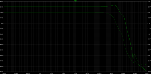
At the beginning of my simulations, the gate resistors have only caused instabilities.
However, after I changed the compensation, the gate resistors made sense again. I interpret this as a good sign.
Now, the stability is not great, but again a little bit better. All my experience with common source at the output had shown something similar. Either high distortion with moderate stability above low distortion, and poor stability.
That's a bit of a challenge
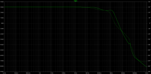
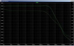
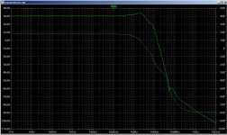
Now, open loop and closed loop with 128mA bias through the mosfets:
However, after I changed the compensation, the gate resistors made sense again. I interpret this as a good sign.
Now, the stability is not great, but again a little bit better. All my experience with common source at the output had shown something similar. Either high distortion with moderate stability above low distortion, and poor stability.
That's a bit of a challenge
Now, open loop and closed loop with 128mA bias through the mosfets:
Attachments
- Status
- This old topic is closed. If you want to reopen this topic, contact a moderator using the "Report Post" button.
- Home
- Amplifiers
- Solid State
- Mosfet-amp module in Class-B