Member
Joined 2009
Paid Member
Folks, those of you that like to optimize, do follow what Michael is going to talk about, he has been looking in more detail at different aspects of the compensation. There may be some improvements worth experimenting with which only involve parts values (topology changes mean you are on off piste as far as the pcb goes). I will be interested to see how well some of the subtleties of the design are revealed by his approach. There is more to the front end of this amp than meets the eye.
Thanks for the help!
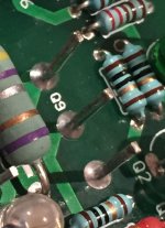
I have the latest revision of the boards TGM8V5B... I think I was one of the last people to order/receive them.
D8 is obviously an SM equiv of 1N4148 (shame it was not in the BOM I used 'cos I don't keep stock of SM parts like this). It looks like its purpose it to enable the green LED to ight up. R39 obs sets the LED current, so the 1K I fitted will probably need replacing by the 750R in the schematic to ensure the LED is bright enough.
Looks like R35 limits the current when it pulls down the base of Q12 in a fault condition. I expect 1K (as I have fitted) would be OK, but I'll probably change it to 4K7 for peace of mind.
I will have to order C25. I have some 22uF tants but they are a bit too big to comfortably fit on the pads.
Folks, those of you that like to optimize, do follow what Michael is going to talk about, he has been looking in more detail at different aspects of the compensation. There may be some improvements worth experimenting with which only involve parts values (topology changes mean you are on off piste as far as the pcb goes). I will be interested to see how well some of the subtleties of the design are revealed by his approach. There is more to the front end of this amp than meets the eye.
I have looked at this from the perspective of keeping the changes down to a minimum.
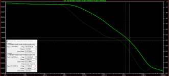
The main issue is the value of C5 is too low at 22pF and this is something that can be tweaked without difficulty to achieve a phase margin of at least -45 degrees.
Unfortunately this circuit is not a two pole compensation scheme as the attached image shows and so the maximum rate of decline for slope between -3dB and unity gain frequency is 6dB/Octave (20dB/Decade). Refer to footnote at end.
With 22pF the unity gain frequency is 1.24MHz at which point the phase has reached -162 degrees leaving a phase margin of 17-18 degrees.
The simplest remedy for existing builds is to increase C5 value from 22pF to 200pF -with a surface mount capacitor it may be possible to do a neat job of soldering an additional 180pF capacitor piggy-back on top of C5. Through hole types will be easy enough to substitute 220pF for 22pF.
For new builds R8 can be omitted while the values for R10 and R5 could be increased to 2.2k and 100R respectively. This would allow a value of 100pF to be used for C5.
In effect C5 impedance is in parallel with 2.2k of R10 - this would reduce the loading effect on Q4 collector slightly - a little more ideal.
I will post some .asc files when I have checked the component numbering against the latest reference model you posted.
Footnote - the image attached to post 456 on page 46 due to bimo has the appearance of a two pole compensation scheme. I have not attempted a simulation of this however there are some differences due to the introduction of Q3 and the folding of R4 into R9 in your circuit.
Attachments
Hmmm, think I might have to refit some parts based on mjona's comments. The additional benefit is that the gain of the amp is also altered to ~23 - which is ideal for comparison with my other amps (in a semi-acive system).
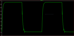
Wish I'd noticed the image in post #523 before. The steps in the positive going waveform are a clear sign of being on the edge of stability IME.
Has this amp been tested with capacitive loads?
Wish I'd noticed the image in post #523 before. The steps in the positive going waveform are a clear sign of being on the edge of stability IME.
Has this amp been tested with capacitive loads?
Member
Joined 2009
Paid Member
I would have to check my notes but I usually test the amps with a small value capacitor at the output in parallel with the resistive load. I didn’t find any problems but perhaps some of you will do more extensive testing which would be of great interest to meHas this amp been tested with capacitive loads?
Unfortunately I don’t have time to dive into the simulations that Michael has been doing so I’m going to let this thread evolve a little bit by itself. I will offer a couple of thoughts that go back to when I did my own simulations and I would encourage those that are interested to do their own simulations as it will teach you a lot about how the amplifier works. it is a lot more complicated than it first appears. The Front and has three transistors and the middle one acts both to buffer the VAS and also to bootstrap the load of the input device greatly increasing in the open loop gain. The compensation at the front end is rather unusual and it was through simulation rather than test and measurement that it was designed. At the time, I looked at it as a form of two pole compensation where the junction of the two compensation capacitors lies at the collector of the middle transistor. I found some advantages to this arrangement in terms of distortion. Then you have the unusual class ABC output stage which has its own local high feedback factor along with parasitic shoot through that is typical of a CFP pair. Optimizing this requires careful attention to the values of various resistors used to set current through the driver devices. The behaviour of this output stage can also affect the waveform of the amplifier under the test. So when looking at the compensation there are a lot of factors being taken into account . I have not yet observed any issues with stability neither have I heard any sound signatures (often unstable amps can have issues in the treble) that imply instability. But maybe you folks can make it even better so it’s very encouraging to see the interest being renewed and the design being examined. I hope this leads to some interesting things.
If you’re worried about building original design I would recommend you just get on with it and get yourself a working amplifier to listen to - those who have done so have enjoyed it.
Last edited:
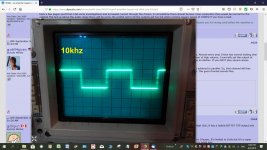
This circuit behaves well enough on a Tian probe plot and on 10kHz square wave with 8R as a load. Unfortunately with increasing capacitance in parallel this induces some spikes in the square waveform which no amount of standing current or frequency compensation is able to expunge. See attached re onset.
Anyway out of curiosity I had run some parallel simulations where the positions of the output BJT's and MOSFET's were swapped around.
This was a suggestion/question that Hugh Dean made in post 10 early in the life of this thread. The point of this was perhaps understated and in the continuing discussions no-one batted an eyebrow.
I had not looked at the lead out details of the MOSFET's to see if these could be interchangeable on the boards with the BJT's - thinking not and it was a bit late to be bringing this up anyway.
Apart from changing some component values the only layout item I looked to change was to connect R7 not to zero volts but to the output line - bootstrapping the collector load of Q3 to make this in harness with Q4.
Implementing the latter would involve at least one hack on the existing boards. I am not a builder but I have run Tian probe plots and a 10kHz test simulation and am happy to post the .asc files.
Attachments
Thanks Daniel for your link and suggestions regarding the ferrite bead. To clarify, it it the 40 ohm value that you recommend or is the value not terribly critical. For my edification, are we wanting to suppress EMI interference or simply provide a variable resistance that varies with frequency to protect the gate? Thanks from all of us who are still learning.
Hi all
Patiently waiting my boards from Gareth - cant wait")
Just trawling through and I thought I would gather a few amendments which I noticed...
Latest BOM doesn't have D8 or C25 listed (added in post #407)... So...
D8 - 1N1418 SOD123 (1n4148W-E3-18CT-ND digikey code)
C25 - 10Uf X7R (1276-1807-1-ND digikey code)
Any confusion over R35 / R39? - R35 = 4K7 and R39 = 750R (also from post #407)
And after 'mjona's wise advise above:
No R8
R10 is now 2.2K
R5 is now 100R
C5 is now 100pf
I'm a total newbie, but thought it may help to have a small consolidation on tweaks
Patiently waiting my boards from Gareth - cant wait
Just trawling through and I thought I would gather a few amendments which I noticed...
Latest BOM doesn't have D8 or C25 listed (added in post #407)... So...
D8 - 1N1418 SOD123 (1n4148W-E3-18CT-ND digikey code)
C25 - 10Uf X7R (1276-1807-1-ND digikey code)
Any confusion over R35 / R39? - R35 = 4K7 and R39 = 750R (also from post #407)
And after 'mjona's wise advise above:
No R8
R10 is now 2.2K
R5 is now 100R
C5 is now 100pf
I'm a total newbie, but thought it may help to have a small consolidation on tweaks
Anyway out of curiosity I had run some parallel simulations where the positions of the output BJT's and MOSFET's were swapped around.
This was a suggestion/question that Hugh Dean made in post 10 early in the life of this thread. The point of this was perhaps understated and in the continuing discussions no-one batted an eyebrow.
I had not looked at the lead out details of the MOSFET's to see if these could be interchangeable on the boards with the BJT's - thinking not and it was a bit late to be bringing this up anyway.
I think the pinout is fine; BCE and GDS would "fit".
However, I don't understand how this could work due to the FET threshold voltage being higher than the Vbe of the output transistor. I.e. if the voltage across R20 is 2V, then the voltage across R20 + R21 must be >2V and the o/p transistor would be in meltdown!
Dave,
By driving the bipolar first, then driving the mosfet of opposite gender from a resistor in the collector of the bipolar at the rail. Really this is just a CFP.
The bipolar would deal with the low voltages, say up to 1A, then with the sense resistor of say 4.7R the mosfet could chime in and pass additional current through drain current onto the emitter of the bipolar. Both could then use the same emitter/drain resistor to the output. You could limit the mosfet current by putting a 4.7V zener across the 4.7R gate/source resistor.
Dave,
By driving the bipolar first, then driving the mosfet of opposite gender from a resistor in the collector of the bipolar at the rail. Really this is just a CFP.
The bipolar would deal with the low voltages, say up to 1A, then with the sense resistor of say 4.7R the mosfet could chime in and pass additional current through drain current onto the emitter of the bipolar. Both could then use the same emitter/drain resistor to the output. You could limit the mosfet current by putting a 4.7V zener across the 4.7R gate/source resistor.
Ah yes, crafty idea.
That's different to what I understood from a few posts earlier (maybe I should have gone back to look at your original posts).
This scheme would require some reconfiguration. The board is rather tight for experimental procedures!
I really should get this amp finished. However i have been distracted by a Hawk A-18 build along with some Rotel amps I seem to have acquired... the wife's black box radar keeps locking on to targets!!
Dave,
By driving the bipolar first, then driving the mosfet of opposite gender from a resistor in the collector of the bipolar at the rail. Really this is just a CFP.
The bipolar would deal with the low voltages, say up to 1A, then with the sense resistor of say 4.7R the mosfet could chime in and pass additional current through drain current onto the emitter of the bipolar. Both could then use the same emitter/drain resistor to the output. You could limit the mosfet current by putting a 4.7V zener across the 4.7R gate/source resistor.
I have reset my simulation as close as I can to the original configuration - that is apart from the component line up and the output stage elements where I tried swapping the positions of the BJT and FET devices. That is as far as I have been prepared to go and it needs someone to have a fresh look.
The simulation is attached. I have increased the spacing around the output stage to ease the congestion for running new connections.
Attachments
Member
Joined 2009
Paid Member
Boards received and look great! Many thanks!!
...Once assembled, I’m not overly sure on testing... where to put the probes and values I need to see and adjust to... any help would be massively appreciated... apart from that, I think I’m ready to solder on!
I am the first to admit that this board is not easy to probe because it’s densely populated and when mounted to a heatsink the underside of the board is not accessible at all. It’s not a beginners project in this regard.
Clearly, you want to assemble it carefully so that you are confident that there are no mistakes. Double check all the parts are the right values and installed properly. Clean the board carefully to remove excess flux from the soldering. I do this more than once during the build as it gets harder to reach all the parts once the board is finished. Look over the board for any solder bridges or small pieces of conductor that shouldn’t be there.
As an additional precaution you can test the board un-powered before it’s mounted on a heatsink. Use a DMM set to resistance mode and measure between each power rail and ground - looking to ensure there’s no dead-short (< 10 Ohms) that would draw excessive current if power was applied.
Before mounting on the heatsink you can also check that the bias potentiometer, VR2, is set to deliver minimal bias - essentially turning the output stage off so that there’s no danger of it drawing excess current on first power-up. Use a DMM on resistance range to probe the terminals of the bias potentiometer and adjust it so that the resistance across pins 1 and 3 is small.
I use a current-limited bench supply for first power up. This allows me to limit the current and voltage and ramp them up, with no load connected to the output of the amplifier. An initial current flow is required to charge the on-board capacitors. If you don’t have such a supply, a trick quoted on the forum is to install a light bulb in series with the power transformer. A mains light bulb in series with the mains supply to the primary of the transformer will glow brightly if the amp is trying to pull too much current (or if the power supply rectifiers are shorting the secondary of the transformer).
Another good precaution is not to install the power rail fuses on the board at first, but temporarily connect in place of each fuse a 100Ohm power resistor instead. This limits the current to avoid damage in case of a fault. By measuring the voltage drop across each resistor you will be able to determine the current draw on each rail using Ohms Law. Anything more than tens of mA is a cause for investigation.
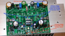
If all is good you can apply full power, with fuses installed. The next step is to set the bias current for the output stage using VR2 and the dc-offset adjustment using VR1. It’s usually helpful to adjust them both in turn, going back and forth between them because the bias is best set when the dc-offset is close to zero. It’s not easy to set the dc-offset, small adjustments are needed and a result of less than 10mV at the output is good enough. The dc-offset is measured at the output with respect to ground. However, because excessive dc-offset will prevent the output relay from closing (the LED will remain red) you may need to monitor the dc-offset before the relay and adjust it until it’s low enough that the output relay closes (the LED will go green). One option for a place to probe the output before the solid state relay is R30 or R31 (blue arrows in attached image). If the dc-offset is within a reasonable range and the LED is green, then probe at the speaker connection which is much easier.
To measure the bias current it’s best to measure the voltage drop across the string R30 + R31; we are aiming for around 50mV to 60mV here (you might see a + or - value depending on which way around you connect the probes). You want to set the bias current by starting from zero and ramping it to somewhere around 30mV and then let the devices warm up slightly and check that the bias remains stable. If it’s not stable we might have a problem somewhere. A convenient place to monitor the voltage across R30 and R31 is show by the red arrows in the attached image.
If you are lucky enough to have two DMM’s you can set one on voltage to measure the dc-offset of the output and the other on voltage to measure the bias current.
Attachments
Last edited:
Member
Joined 2009
Paid Member
Advanced Option: One thing I’ve beed doing on other builds is to install the power transistors and leave their leads at full length, poking up above the board so that I can probe them directly, or even tack on small insulated wires using my soldering iron and use these small wires to connect to the multimeter and avoid putting any probes on the board at all - much safer if, like me, you’ve blown an amplifier up when a meter probe slips !! (the attached image shows an example of the leads poking up, this is from my TGM1i amplifier but the idea is the same)
Attachments
Last edited:
I’ve been looking on here for a power amp project, and after watching this thread from the shadows, I decided to go for it. I had some PCBs made, using the published gerbers, and built two amps. Powered each one up on the lab PSU and, bingo! They both worked first time and the DC offset and bias was very stable. I mounted the pair of them on a plate, with heat sinks and wired them up to a SMPS300 at +-36v just to try. Right away the sound had such authority and pace but in a relaxed and musical way with a softness in the upper registers. All was well until the busy bee noises started. Looked like the SMPS wasn’t happy with the 20mF/rail. Anyway I now have a high quality transformer from Tiger Torroids. This is providing 35-0-35 ac (400VA ) and +/- 53V with a single 25A bridge rectifier and no additional capacitors. I now have a very powerful amp with huge scale but is seems slower and less lively than with the SMPS. Any recommendations on the best way to wire a pair of TGM8s to a single transformer would be appreciated. I’m listening as I write so I’m off to turn the volume up... just a little. Gareth thank you for a great project and your guidance.
Geoff S.
Geoff S.
Member
Joined 2009
Paid Member
Hi Geoff,
Glad to learn that you are having fun. Interesting that you hear the differences between psu types, I’d like to try that myself some day.
For single trafo, you can also employ a pair of bridge rectifiers (not a single one like you have now), using one for +ve rail, one for -ve rail and then hook the rectified power rails to the left and right channels in parallel. I didn’t compare all the options, like having separate bridge rectifiers for each channel. So, sorry, can’t recommend a ‘best’ approach from a sonic point of view. If you are in the mood to experiment then I’d encourage you to trust your ears on the best arrangement.
Thanks Gareth, I'll try a few things to provide some isolation between the two amps. Fig.2 here.. Power Supply for Power Amplifiers is what you suggested. I might try this without caps, smaller caps, possibly series 0.1R in the output rails.
- Home
- Amplifiers
- Solid State
- TGM8 - my best amplifier, incredible bass, clear highs, no fatigue (inspired by Rod Elliot P3a)