I opened the schematic and started hyperventilating!! What happened to the design in post #1 ;-) Seriously though, this could be a good basis for experimentation if you end up organising a group buy...
One option I don't understand is offering The choice of both TH and SMT parts for the compensation caps. Unless there is a sonic difference why not just pick one or the other and save some board space?
The only error in the schematic that stands out to me is the lack of some 4,700uF caps on the rails ;-)
Member
Joined 2009
Paid Member
It's OK, I fixed it, see, ")
The reason to offer through-hole for the compensation caps is because some folk believe only silva-mica will do and anything else is a problem. However, for others who are happy that np0 ceramic is a superb quality capacitor and readily available in SMT I give a choice.
The reason to offer through-hole for the compensation caps is because some folk believe only silva-mica will do and anything else is a problem. However, for others who are happy that np0 ceramic is a superb quality capacitor and readily available in SMT I give a choice.
Attachments
I prefer to think of it from the other end..........It depends on the amplifier and the source. I have seen many people report that the input cap is critical and so small on-board caps can be a compromise. As a result, you need to allow lots of board space for high end film caps. Or you mount them off-board. The SKA GB150 by Greg has space for a small on-board cap and most people don't install it...............
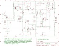
The Power Amplifier input needs a DC Blocking capacitor, or some other arrangement.
The Designer/Builder of the Power Amplifier knows the required Passband of that amplifier and can make an informed decision on what size of DC Blocker to install or not. i.e. set the F-3dB frequency ONCE for this Power Amplifier and know that ALL Sources are safe to use with this Power Amplifier.
Buy and fit ONE good capacitor and the "problem" is solved.
Any Source can be used, whether it has an output offset, or not. Any lower quality DC Blocking cap in any Source can be shorted out and the Builder knows his speakers are safe.
Do it ONCE where you know what is required.
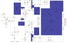
R2 does not need to be "glowing". Use smt 1/8W and bypass with a pair of inverse parallel rectifier diodes to conduct Fault Current to PE..........Eagle schematic. .......... I've determined which resistors need to dissipate reasonable power and have shown them as 'glowing resistors' on the schematic. I am going to favour through-hole parts for these resistors and SMT for the rest............
The worst case Vf during Fault Current will be around 1Vf to 3Vf.
The worst case transient dissipation on the resistor is limited by that Vf.
Pmax transient peak <= 3^2 / 10r = 900mWpk. A metal oxide (thick film), or metal film (thin film), smt will survive this transient.
If the mains fuse does blow due to a mains fault passing this diode protection, then it is worth replacing both the diodes and the resistor. Or at least check they are still working !
Last edited:
Fixed what? All I can see is tiny 330uF caps on the rails
Anything bigger won't fit on a small pcb with limited dimensions. For onboard caps 330uF is enough.
Last edited:
Member
Joined 2009
Paid Member
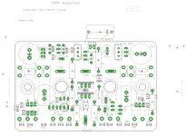
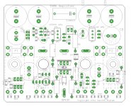
I've created a first draft of the pcb layout. It's currently 92mm x 60mm double sided. It may be that I have to start-over with a different concept but this version follows the same style as my TGM7. The power devices are sandwiched between the pcb and heatsink (with washers to isolate back of pcb from power devices) so the footprint is entirely that of the pcb. I've used wide traces where there's significant current, put the drivers right up near the power devices, put the Vbe multiplier back-to-back with one of the drivers (thermal contact), kept the power and power ground close together so the wires can be twisted.
But as you can see, there's no room for an input capacitor as drawn. I can make the pcb another 10mm or 20mm wider to accommodate an input cap but I'm not sure I wouldn't prefer to mount it off-board.
p.s. I renumbered the schematic using the Eagle 'renumber' tool.
But as you can see, there's no room for an input capacitor as drawn. I can make the pcb another 10mm or 20mm wider to accommodate an input cap but I'm not sure I wouldn't prefer to mount it off-board.
p.s. I renumbered the schematic using the Eagle 'renumber' tool.
Attachments
Last edited:
Member
Joined 2009
Paid Member
And if we did stretch the board to 75mm tall we can squeeze on the input capacitor and two pairs of rail capacitors. For 63V rated caps you can get up to 1,200uF, and for 50V rated caps it's relatively easy to get 2,200uF per can. Together with the electrolytics that are mounted up close to the output device pins this would get you to 4,700uF per rail. The grounding layout isn't working so well as the extra rail caps tie in to the power ground asymmetrically although all the signal grounds are well separated. I'll give some thought as to whether this is actually an issue or not since the caps next to the power devices are closely tied to star ground and will decouple the rails fairly well.
Attachments
Last edited:
Hi Bigun
There appears to be a lot of empty space on and around the power transistors. You've put the caps there and I can't help but wonder if they'd be better elsewhere? What footprint are these caps they seem quite large for 330uf.
I know I asked for filter caps onboard - and that is still my preference - but I prefer the first layout. Is there any way to work within the approx. dimensions of the first layout, reduce the amount of "whitespace" and have enough room for an input cap? I think onboard filter caps would be of far less interest to most constructors than the input cap - even if there is only enough room for an MKT or similar with 5mm pin spacing.
The other thing worth exploring is moving the output transistors to the edge of the board like on the DX Blame MkIII. Constructors could either opt to lie them flat to flush mount the board on the heat sink, or at 90' so the board is affixed to the bottom plate. That should free up some board realestate for trace layout. Although I kinda like the underboard because that's how Rod does it with his P3A and other power amps...
Alternatively, get rid of the MOSFETs
Last edited:
Member
Joined 2009
Paid Member
Hi Rachu32 (do you have a regular name ?),
I'm quite prepared to try some other layout options.
What I have created so far is to show that it's possible to put it all on one board, based on the layout I used for TGM7. We have all the optional pieces, enhanced VAS, MOSFETs, solid state relay with dc-protection + delay-on and fast-off, with the power devices under the board. The white space you see is needed for the wide traces to carry high currents - actually if you look closely at the first image in post 67 you'll see there is very little unused space around the power devices. It is necessary to leave clearance around the mounting holes of course.
The smallest board possible would only have the basic amplifier, no output relay and with single pair of power devices at the edge as you suggested and perhaps even the fuses moved off board to the power supply - it could be compact indeed.
I'll give some thought to the alternatives...
Ivanlukic, yes, more options is good, and the bigger the board the better - so long as the space is properly utilised.
Bigun, what size are the pads for the main filter caps? 4700uF /rail is more than adequate. I'm more concerned that there is enough space to accommodate large caps that can take up the ripple.
Also the board height should ideally be 74mm so it can be flush mount to the back of a 75mm heat sink.
Bigun, what size are the pads for the main filter caps? 4700uF /rail is more than adequate. I'm more concerned that there is enough space to accommodate large caps that can take up the ripple.
Also the board height should ideally be 74mm so it can be flush mount to the back of a 75mm heat sink.
Member
Joined 2009
Paid Member
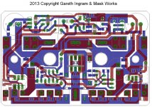
The routing doesn't make the additional filter caps a great addition. The ground return for the +ve rail filter caps would have to be routed back through the ground return for the -ve rail filter caps before reaching star ground. This wouldn't be a design to be proud of. I'm thinking to myself that the main benefit of putting them on board would be if I wanted to put the whole power supply on there - and the board is too small for that. So for now I'm not sure that there is a good way to include all that unless you fellas want to send me the purchase price for an unrestricted version of Eagle. Or unless we strip out circuit functionality - it might be fun to make up a small board with a minimum of functionality.
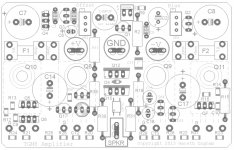
So before I consider stripping out stuff I thought I'd first see if I can 'finish' off the current version by looking at trying to squeeze an input cap into the current version of the layout. However, don't get excited, it's a small space. I've put on a footprint for an electrolytic with 5mm pin spacing and a 10.5mm diameter. This is also compatible with a film capacitor with a 5mm pin spacing with a size that would fit inside 7.5mm x 7.5mm. It's enough space for a small film cap, say a 1uF metalized polyester. If you want a really high end film cap with lots of capacitance it's best take it off board or we have to make the board bigger - just for the cap (we could do this).
But the footprint I've used is enough space for a bipolar electrolytic of at least 10uF. Don't puke, this isn't such a crazy idea - it will minimize the phase shift of the input filter at low frequencies and some have found them to sound very good. I could add a footprint for a small SMT bypass cap too.
http://www.diyaudio.com/forums/solid-state/44659-input-capacitor.html - read post #34.
Attachments
Last edited:
I like this revised layout very much. The input cap is nicely placed with space for a 10uF polyester or high quality 10uF electro. That should please virtually everyone.
While I would have to put the bulk caps onboard to simplify chassis wiring, I would prefer to omit them from the board entirely unless there is enough space for the complete supply. I.e. it just adds cost and complexity to have some mounted offboard and the rest onboard. You've already taken care of the local filtering with 330uF, noting that is already more than the 100uF Rod specifies.
Personally I would be happy to omit the advanced VAS and MOSFETs since they are of no particular interest, if it meant it freed up enough room for a robust cap bank. But I suspect that the vast majority of people interested in this layout would prefer to experiment with these features and would be perfectly happy to construct a separate cap bank. So on that basis I consider this layout very good indeed!
Sent from my iPad using Tapatalk
What worries me is those electros on and around the output transistors. When the outputs are sandwiched like this the board tends to heat up quite a bit. This was the other reason I suggested earlier that placement of the outputs at the top edge of the board might be better solution. The others are to free up board space for components and/or traces and giving more transistor options. If the boards are manufactured plated through hole, and the transistor legs are inserted from underneath and soldered from the top, flush mount assembly is very easy.
Alternatively, perhaps careful separation and specification of 105C caps would be sufficient for long term reliability. I'm not sure how big of an issue it is. Probably more so with the FETs and higher voltage rails.
Sent from my iPad using Tapatalk
Alternatively, perhaps careful separation and specification of 105C caps would be sufficient for long term reliability. I'm not sure how big of an issue it is. Probably more so with the FETs and higher voltage rails.
Sent from my iPad using Tapatalk
Member
Joined 2009
Paid Member
I'm going to give some thought to an alternative layout with fewer options but with filter caps on-board.
In terms of the sandwiched idea - I did do as you say, put the hot power devices right in contact with the underside of the board on my TGM5 project. It wasn't an issue and it made the board really stable. However, I am not proposing that idea here - rather there should be some spacers/washers between the power device and the pcb. In fact I have crammed so many parts on the board that there must be a gap underneath to accommodate them all. This will take care of the heat issue. But the best solution is to keep the large cap back away from the heatsink altogether.
In terms of the sandwiched idea - I did do as you say, put the hot power devices right in contact with the underside of the board on my TGM5 project. It wasn't an issue and it made the board really stable. However, I am not proposing that idea here - rather there should be some spacers/washers between the power device and the pcb. In fact I have crammed so many parts on the board that there must be a gap underneath to accommodate them all. This will take care of the heat issue. But the best solution is to keep the large cap back away from the heatsink altogether.
Member
Joined 2009
Paid Member
I haven't thought that far ahead but I plan to order a prototype run of boards which will allow me to build the thing and see if it works; the minimum buy is 10. Not much point worrying about a group buy until the design has been validated though and since most folk are allergic to surface mount parts I wasn't expecting to go much further than make some boards available to a few interested folk from this thread.
Anyhow, the current version of the layout, let's call it the 'Full Monty' is ready to go - if anybody believes the design is fault-free and wants to take the risk and pony up for the prototype board run ($35 or so) rather than wait for me. It's designed to be good for more than 100W with 50V rails. It's aimed to compete with the TGM7 for my home theatre.
However, I'm going to think about the simpler version before I jump in, the simpler version will be aimed at a lower rail voltage.
Last edited:
That is an excellent price for such a small run. May I ask which board house you are using?
If 'simpler' and 'lower power' means a layout without the MOSFETs then I would be more interested in waiting for that Rather than reducing the board size (a rather pointless exercise since it's so small already) can you make this one with sizeable onboard filter caps? Or alternatively a stereo board?
Provision for the input cap and DC protection should be included in every layout IMHO since they occupy little space and are useful. The enhanced VAS less so... but because it takes up hardly any space either I'm indifferent to that.
Happy to pay half the cost of a board run plus shipping from your place to mine.
Sent from my iPad using Tapatalk
If 'simpler' and 'lower power' means a layout without the MOSFETs then I would be more interested in waiting for that
Rather than reducing the board size (a rather pointless exercise since it's so small already) can you make this one with sizeable onboard filter caps? Or alternatively a stereo board?Provision for the input cap and DC protection should be included in every layout IMHO since they occupy little space and are useful. The enhanced VAS less so... but because it takes up hardly any space either I'm indifferent to that.
Happy to pay half the cost of a board run plus shipping from your place to mine.
Sent from my iPad using Tapatalk
But the footprint I've used is enough space for a bipolar electrolytic of at least 10uF. Don't puke, this isn't such a crazy idea - it will minimize the phase shift of the input filter at low frequencies and some have found them to sound very good. I could add a footprint for a small SMT bypass cap too.
http://www.diyaudio.com/forums/solid-state/44659-input-capacitor.html - read post #34.
I completely agree with Owdeo about the sound of electrolytic input cap. To me it sounds better than the best and most expensive film caps. I did not know about this thread but I reported my experiences in Fet Hex explendit thread and was somewhat surprised that Gabor Bela confirmed my opinion. Therefore it is better to use higher value (bipolar) elco than lower value film cap. But since it will be usually exposed to very low voltage it may be desirable to form it (with battery or suitable DC voltage) before soldering to the pcb.
- Home
- Amplifiers
- Solid State
- TGM8 - my best amplifier, incredible bass, clear highs, no fatigue (inspired by Rod Elliot P3a)