Thru-hole connections to wide PCB traces like power buses usually have a thermal pad to make it easier to solder.
What's the practice with SMT components?
Typical application would be an SMT emitter resistor to a wide output trace or a substantial SMT capacitor between earth and the positive rail.
Most of the SMT recommendations I can find are oriented to much smaller applications.
Best wishes
David
What's the practice with SMT components?
Typical application would be an SMT emitter resistor to a wide output trace or a substantial SMT capacitor between earth and the positive rail.
Most of the SMT recommendations I can find are oriented to much smaller applications.
Best wishes
David
Thermal relief does make SMD easier to hand-solder. Without it, if the pad is part of a large copper pour, you'll need a decent tool (like 50W soldering iron with temperature control), with a 20W iron and a skinny tip, it'll just get stuck.
Same for sticking vias in pads.
But it has less inductance and resistance. A few mm of skinny trace is enough to make a decoupling cap between power and ground planes useless, so, your choice.
If it's a part which will disispate some heat, like a LDO or a power resistor, the copper pour becomes a very useful heat sink. In this case, using thermal reliefs defeats the purpose...
If you use reflow soldering in an oven, it heats the whole board, which makes it less an issue.
Also many SMT recommendations aim to have a smooth volume production, for example using via-in-pad cools the pad during soldering and sucks up the solder, which is why it's not very common. The vias usually need to be plugged first with ca conductive filler. For DIY, you usually don't care about that, if that particular pad takes a little longer to solder by hand or needs a little bit more solder, who cares.
Last edited:
Agree with this. SMD soldering is something I do everyday at work.
Having a 50W soldering iron and using plenty of flux there is no problem with large copper areas.
You can use a normal cooking oven for SMD. Just need to use a thermocouple in there to make sure you are using the correct process temperatures.
Having a 50W soldering iron and using plenty of flux there is no problem with large copper areas.
You can use a normal cooking oven for SMD. Just need to use a thermocouple in there to make sure you are using the correct process temperatures.
Member
Joined 2009
Paid Member
To avoid a cold joint you want to ensure that the chip's solder heatsink and copper plane are both hot enough for the solder to flow properly. If there's no exposed land I'd suggest first pre-soldering the land area to cover the pad with a reasonable thickness, then place chip over it and heat the combined area through the heatsink to melt the solder. Usually it isn't recommended to do this and instead to use only fresh solder but I've not found a way to avoid this method if the landing area is (improperly designed) hidden by the part. On the other hand it appears to work well.
If the landing area is larger than the part then I usually treat it like a through hole joint and place the tip of my iron on the landing area but then slide the tip up against the lead of the part you are trying to solder so that you heat both the landing area and the part at the same time. Soldering the larger SMT parts can be as easy or easier than through-hole parts, requires no lead clipping, uses less solder and leaves less flux residue plus is easier to clean.
I don't glue SMT parts before soldering them so in some cases I might choose to 'tack' a part on to the board lightly soldering one of the leads to it's pad with a 'touch' of the iron and then carefully solder the remaining leads one at a time, then come back to the first one and solder it more thoroughly. This works well with power transistors where you tack the small signal leads to hold it before soldering the heatsink.
It's bad practice to use pads that are undersized for soldered heatsinks - check the data sheet for the part - the pad area is an important and integral part of the heatsinking and needs a large enough area to work. In my TGM5 amplifier (thread around here) I even added additional pieces of copper to the heatsink of SMT power devices to increase copper area and heatsinking without using up additional board area.
You still need to be careful you don't overhead a part whilst soldering it which is where a powerful iron helps because it allows you to complete the joint quickly.
N.B. This is just my approach - I have no SMT training or experience other than applying what I think is common sense to my hobby projects.
Last edited:
Does one place the 50W iron on the copper plane next to the chip's solder heatsink? or on top of the chip's solder heatsink?
What if there is no exposed land next to the chip's heatsink lead?
Usually I would apply heat on the copper plane, that way the molten solder works as a very efficient heat transfer media.
When there is no exposed plane, it would require using a hot air rework station. I once tried with a heat gun mounted on a stand to help preheat a heat sink before soldering it. It helped but not as much as I had thought it would.
...When there is no exposed plane, it would require using a hot air rework station...
I have not used a proper hot air rework station.
It's called a "rework" station but I wondered if it would be a better way to solder to a plane.
Perhaps I could preheat the copper with my paint stripper/hot air tool.
Any one here with experience in either technique?
Best wishes
David
SMT layout
I bought a sparkfun hot air, it worked much the same as a Hakko that I used in the past. Just have to get the right nozzles for the application.
When I do a copper area fill, I just let it do it the same as a through hole or via. You can adjust the thermal gap width to make more contact to the PTH.
For
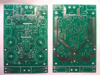
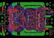
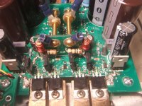
I have a LME49830/LatFet amp in the works and am using Ohmite FCSL R's as ballast R's, so that I can measure the current. The FCSL are on the right side, I have 2 pairs of TO-264 to be mounted on the backside, LME is on the left side. See attached.
I bought a sparkfun hot air, it worked much the same as a Hakko that I used in the past. Just have to get the right nozzles for the application.
When I do a copper area fill, I just let it do it the same as a through hole or via. You can adjust the thermal gap width to make more contact to the PTH.
For
For this I do not do a copper area fill/pour, I do a full contact (copper area) with no thermals and then crank up the temp on the weller and put a wide chisel tip on it.Typical application would be an SMT emitter resistor to a wide output trace or a substantial SMT capacitor between earth and the positive rail.
I have a LME49830/LatFet amp in the works and am using Ohmite FCSL R's as ballast R's, so that I can measure the current. The FCSL are on the right side, I have 2 pairs of TO-264 to be mounted on the backside, LME is on the left side. See attached.
Attachments
Last edited:
The only reason I would include a SMD pad inside a copper pour is to heat sink the device via the SMD pin such as the collector or drain of a transistor. Otherwise I leave a small 'leader' coming from the pour and forming the SMD pad. If you assemble with a soldering iron that is too hot you risk lifting a pad or causing thermal fatigue to the SMD pins and internal bonding wires that connect to the die. If you bury a 0201 or 0402 or something small like a SOT-563 pin inside a pour, you will have trouble soldering by hand for sure. For example, in my EC mosfet amp there are many different size SMD packages used, even 0201 resistors and 0402 X 4 resistor arrays all soldered by hand.") SOT-23 is a relatively large component for me.
SOT-23 is a relatively large component for me.
SOT-23 is a relatively large component for me.Attachments
Last edited:
...The only problem is the potential for overheat...
I would use a proper temperature-controlled hot air rework station.
I just checked one and found the hot air unit is 300 W.
I wonder if that would that melt solder on a copper plane better than a 50 W iron, once inefficiencies are allowed for?
Best wishes
David
...For this I do not do a copper area fill/pour, I do a full contact (copper area) with no thermals...
What is the difference for your layout between "a copper area fill/pour" and "a full contact (copper area)"?
Best wishes
David
For big stuff like D2PAK, with vias underneath for heat sinking, I use this method :
- oversized pad (to have room for the soldering iron tip) and pre-tin it then flux, or apply solder paste.
- place component
- heat the pad with 100W soldering pistol
It is very quick, I heat mostly the pad and the heat is transferred to the component once it sits in a molten solder bath. The ground plane sucks up the heat very efficiently, so a lot of power in little time is best. It is useful to have an oversized pad to put the pistol tip.
Cooper area fills/pours make thermal reliefs, where as a cooper area is full contact,no thermals. This terminology is dependent on the CAD SW that you use. and what are you using for CAD SW?What is the difference for your layout between "a copper area fill/pour" and "a full contact (copper area)"?
The hot air allows more heat to cover a larger area, thus is more effective in my mind.I wonder if that would that melt solder on a copper plane better than a 50 W iron, once inefficiencies are allowed for?
... is dependent on the CAD SW that you use. and what are you using for CAD SW?
As you say, dependent on the software so I wanted to confirm.
I have DesignSpark, and you?
The hot air ... is more effective in my mind.
I suppose I will just have to try a few experiments.
The people with hot air systems seem enthusiastic about them so it seems worth a try.
Best wishes
David
I have DesignSpark, and you?
I suppose I will just have to try a few experiments.
The people with hot air systems seem enthusiastic about them so it seems worth a try.
Best wishes
David
You should have no problems with a temperature controlled hot air system. You can pre heat the pad long before adding the components. I have had no problems with melting the solder on the pads before adding the component. A little "no clean flux" on the component legs allows the solder to flow nicely(This is not always required but some parts are stubborn, water based flux can spit). Not tried this method on fine pitched ICs though. Drag soldering works well for these.
PS. Design spark is good but a little unstable in my experience.
Last edited:
... [useful comments]...
PS. Design spark is good but a little unstable in my experience.
It seems pretty decent but I don't have sufficient experience yet to comment on stability.
The component library does not include the transistors I use, of course.
Next step is to learn how to add ThermalTrak transistors to the library.
Thanks for the comments.
Best wishes
David
ORCAD16.0 for the stuff, I posted. It barely does the job, but is stable. I do like to use GerbTool to check gerber/drill data just to be sure it comes out correctly.I have DesignSpark, and you?
but I have used others as well, Cadence Allegro,Mentor BS.
Having good libraries is important and can amount to a lot of time spent.
Creating new device in Eagle.....
For Eagle, you would go to the sch page @ top menu and click library for the drop down field. Choose 'open' and select the library file to open. ex, Transistor Power file, then in the new window that pops up, go to 'symbol'. Select the symbol you want or type the name of a the new symbol you want to use. (caps only) "Create new symbol 'name'?" pops up. Choose yes.
Draw out your new symbol such as a BJT and diodes that are part of the Thermatrak. Add the pins from the left menu to the symbol drawing. Save. Then go to the ’package’ menu at the top. If the package is not already created, type in a new package name. "Create new package 'name'?" pops up. Choose yes. Draw out the new package and add the pin pads or through hole vias at the proper location. Save. You may need to adjust the grid to the proper scale for whatever package you are creating. Consult the datasheet for the dimensions.
Go to the ‘device’ menu at the top. Create new device by typing in the component number. "Create new device 'name'?" pops up. Choose yes. Go to ‘add’ menu at the left side of the screen and choose the symbol that you just made from the list. On the right side of the screen within the package field, choose ‘new’. Select the new package you just created from the menu. Only packages with enough pins that coincide with the pins in the symbol drawing will be valid. Next select the ‘connect’ button. In the field that pops up, connect the proper pins to the package pads or through hole vias. Save. Close the library and go back to the sch page. Make sure the library you just edited is used. If it is not, then in the ‘library’ pull down menu at the top, click ‘use‘ and choose the proper library file. You should now be able to get to the newly created device from that library under the ‘add’ button at the left side of the screen. Hook up the pins one by one in the sch drawing so that you can verify in the brd drawing that the pin connections are correct. If not, go to the 'library' pull down field and re-open the library file again. Go back to the device menu and choose the name of the device to edit. Click ‘connect’ button in the package field and re-adjust the pinout. Close the library edit page. You have to re-use the device from the ‘use’ button at the left in the sch page in order to update the changes to the device in use.
If you have to make several new devices for the library, make sure you save a backup of the library directory in the program folders…..off site backup preferably.
It seems pretty decent but I don't have sufficient experience yet to comment on stability.
The component library does not include the transistors I use, of course.
Next step is to learn how to add ThermalTrak transistors to the library.
Thanks for the comments.
Best wishes
David
It has loads of parts but not the ones you want.
One thing to watch out for is creating new footprints with similar names (to original default parts) but in different libraries. It seems to want to default to the original part that it came with.
You should have no problems creating new parts. Can try to assist you if you get stuck it on anything. Have used DS quite a bit and have got PCBs successfully made using it.
Paul
- Status
- This old topic is closed. If you want to reopen this topic, contact a moderator using the "Report Post" button.
- Home
- Amplifiers
- Solid State
- SMT connection to copper pour?