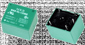
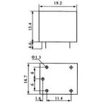
Standard type relays used for audio should be rated within their DC rating, which is a lot lower than their AC rating. They may work fine for many years if all they are required to do is function as a delay for anti-thump. However, if they really do have to protect the speakers when there is a serious fault, the contacts of standard relays may weld together, which means disaster.
If you can't find their DC rating or it is below the rail voltage, you will be gambling with false protection.
If you can't find their DC rating or it is below the rail voltage, you will be gambling with false protection.
Sometimes this type is used too.
thank you mister farjon
")
best regards
Juan
Does anyone have any suggestions for finding some information on Ground Plane layout?
Practices, techniques and examples. Especially with STAR ground layouts of Power Amps.
Using Sprint layout or other products. which is the better or best?
Also has is anyone willing to share techniques, like this one.
Create a Sprint Layout drawing with 100 resistors on it numbered and ready from 1 to 100 the same for caps and diodes. Then insert them and put the value in as you do the layout. This is created ahead of time. Just a tip.
Does anyone have any suggestions for finding some information on Ground Plane layout?
Practices, techniques and examples. Especially with STAR ground layouts of Power Amps.
Using Sprint layout or other products. which is the better or best?
Also has is anyone willing to share techniques, like this one.
Create a Sprint Layout drawing with 100 resistors on it numbered and ready from 1 to 100 the same for caps and diodes. Then insert them and put the value in as you do the layout. This is created ahead of time. Just a tip.
Wish to hear some techniques from the Masters Alex mm and Juan Vargas....
Oh mister Krsifr I did search for that information too but I know that mister Alex MM and OS also knows ways to do it I hope they can read this and show examples of star GND on power amplifiers here an image of one of many designs he made and this is really interesting that all GND are concentrate in that spot.
But depends on the circuit too
Regards
Juan
But depends on the circuit too
Regards
Juan
Attachments
![DADO-TT-TMC-7-2-g-2.LAY].jpg](/community/data/attachments/357/357382-5f7e11b9e70315f2891146da37768d83.jpg)
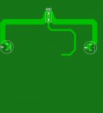
this is really interesting I never thought about having a second layer where GND can be place on top ? this is a nice tip by wire or double side PCB really nice indeed thanks dadod
Regards
Juan
You've got it very well.
Regards
Damir
So I am on the same page, are the ground and the star ground AND the GROUND PLANE "all" the same in that there is no resistive difference? And of course there is SIGNAL ground and maybe a front end ground.
There was a picture of a board on "the best amplifier I ever heard" thread that showed a Goldmun board with a ground plane under the components on the top side of the board. That is the so called shielding I seek, IF it is superior to other layout techniques. Working out THAT technique has eluded me in Sprint Layout, to any consistency.
If it does not help, then I am for not pursuing it.
I hope this discussion will be fruitful to all....
So I am on the same page, are the ground and the star ground AND the GROUND PLANE "all" the same in that there is no resistive difference? And of course there is SIGNAL ground and maybe a front end ground.
There was a picture of a board on "the best amplifier I ever heard" thread that showed a Goldmun board with a ground plane under the components on the top side of the board. That is the so called shielding I seek, IF it is superior to other layout techniques. Working out THAT technique has eluded me in Sprint Layout, to any consistency.
If it does not help, then I am for not pursuing it.
I hope this discussion will be fruitful to all....
Khris I would not go for a ground plan, it could be tricky if not done perfectly as it can introduce stray capacitances and spoil the compensation. Ground plan is actually not needed for audio, it is more used in high frequence circutry.
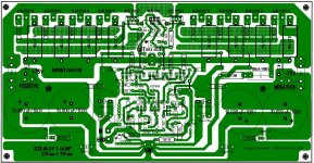
This one example of my TT amp PCB. As it is single sided it uses a wire to connect the grounds and run that wires over power tracks. Better if it is done with double sided PCB
BR Damir
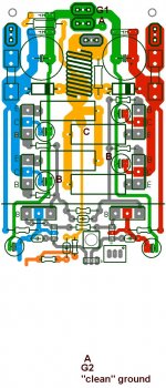
Same thinking here (below 1). Like a kid .. I use colors to visualize the "travels"
of the current pulses back to my dedicated "dirty ground".
Of course , the small signal area has it's own child star which will connect to
the center point of the "dirty" (main star -A/G1 .. below 1 and 2).
Grounding is of the same concept as the centered NFB takeoff point.
In the 1st attachment , I REALLY wanted to (totally) separate the high
current section from the LTP's (2 of them). Also , it is a triple OPS ....
much more "picky" than your basic EF2.
PS - ground plane = big antenna ...
OS
Attachments
 pulled out some copyrighted materials...do not post another's design unless you have permission to do so....
wow! Willy you gave me goose bumps nice man I was practicing today with a Classic one Dx Blame ST
I never get tired of Carlos designs here is a image I just stared today
I notice your skills are more nicer I like that bro let get some cold soda pops jejejejeje
hold on ????? that the B500 from mister Apex ? wow
Regards
Juan
I never get tired of Carlos designs
here is a image I just stared today I notice your skills are more nicer I like that bro
let get some cold soda pops jejejejejehold on ????? that the B500 from mister Apex ?
wowRegards
Juan
Attachments
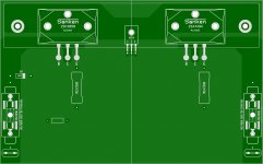
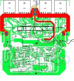
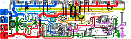
You have kept the +ve, -ve and Power Ground supplies close coupled, good.
You have rail to output diodes, good.
See if you can find space for rail to ground diodes. These should also be after the fuses.
Can you find room to fit HF decoupling (x7r, 100nF to 220nF) to each output device?
Maybe add a few MF decoupling per two pair of output devices.
Move your NFB tapping to the ACTUAL output trace. Even if you have to use a link to reach over that U shaped emitter resistor rail.
- Status
- This old topic is closed. If you want to reopen this topic, contact a moderator using the "Report Post" button.
- Home
- Amplifiers
- Solid State
- Dx Juan layouts ideas PCB