
This is what I meant.
When I increase them.. N channel is 3.9, p channel 50. Offset close to zero,
Temperature both vas transistor 36 deg c
When I try to increase them it will shoot up to 48
Also 550 560 is matched. Closest 5 percent
1381 3503 matched as well
470 ohm checked
Short d1/d2 junction to speaker output checked.
Last edited:
The VBE of your transistors is unusually high and quite different from each other...according to datasheet it should be about 0,65v at 25C and less at higher temperature. Unless your meter is reading also AC oscillation (check in AC reading mode) in addition to DC, I suspect bad transistors...
Fab
Fab
The VBE is intrinsic to the transistor parameter and must match 0.65vdc or so at the collector current it is used.
Are you measuring the transistor VBE directly at the B and E transistor leads?
This will remove the pcb tracks of the equation. If you are sure your parts are good then look at the pcb tracks damage or solder bridge or cold solder....
Fab
Are you measuring the transistor VBE directly at the B and E transistor leads?
This will remove the pcb tracks of the equation. If you are sure your parts are good then look at the pcb tracks damage or solder bridge or cold solder....
Fab
Last edited:
Hi AnthonyA
The input transistors vbe matching has a very small effect on the overall bias values difference unless one of them is defective...
DC Offset stability should be reached quickly with bjt inputs....
As indicated previously ensure you do not measure AC voltage on top of DC voltage....
Can you post an annotated schematics with all voltage measurements and your closed loop connection shown.
Fab
Doesn't make sense then.. I checked all the parts in pcb.. There is nothing wrongly installed.
It starts 50mv offset and slowly drift to 0.01 by 10 mins pretty stable.
The only diff is I connected the ground of capacitance multiplier to ground using a ground break
I got a bad feeling is a bad pcb design as I contacted the local seller and he have zero answer or help
It starts 50mv offset and slowly drift to 0.01 by 10 mins pretty stable.
The only diff is I connected the ground of capacitance multiplier to ground using a ground break
I got a bad feeling is a bad pcb design as I contacted the local seller and he have zero answer or help
Last edited:
Bias different both side .. Pnp is 60mv npn is 140mv
550c and 560c is hfe matched
139 140 vbe matched
J112 matched idss
DC Offset ok no drift after 10 mins.. From 50mv to 0.0x.over 10 mins.
I connected the ground of the supply to ac ground with ground break that became stable. Previously it was a little unpredictable while biasing
Good thermal contact
Voltage stable. As using cmbjt
It's a local pcb.. They Copied the design and made pcb for diyer


Should I carry on or just scrap this project? Doesn't add up..
550c and 560c is hfe matched
139 140 vbe matched
J112 matched idss
DC Offset ok no drift after 10 mins.. From 50mv to 0.0x.over 10 mins.
I connected the ground of the supply to ac ground with ground break that became stable. Previously it was a little unpredictable while biasing
Good thermal contact
Voltage stable. As using cmbjt
It's a local pcb.. They Copied the design and made pcb for diyer
Should I carry on or just scrap this project? Doesn't add up..
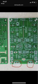
There is at least a fatal mistake on the pcb layout. The output transistors (N and P channels) have the same pin out but on the pcb the speaker output is connected to source on one transistor and on drain on the other one....
I do not know about the rest of the pcb layout but I would not have much confidence...
Fab
I do not know about the rest of the pcb layout but I would not have much confidence...
Fab
Attachments
- Status
- This old topic is closed. If you want to reopen this topic, contact a moderator using the "Report Post" button.
- Home
- Amplifiers
- Solid State
- VSSA Through-Hole-PCB build thread